L9216B/H
Preliminary Data Sheet
September 2001
High-Voltage Ringing SLIC with Ground Start
Supervision (continued)
80
60
Tip or Ring Ground Detector
40
In the ground key or ground start applications, a com-
mon-mode current detector is used to indicate either a
tip- or ring-ground has occurred (ground key) or an off-
hook has occurred (ground start).
20
0
–20
–40
–60
–80
For ground start applications, detection may be seen at
the output of the common-mode current detector
(RGDET) or the loop closure detector (NSTAT).
0.00 0.04 0.08 0.12 0.16 0.20
0.02 0.06 0.10 0.14 0.18
TIME (s)
If ICM is used, the detection threshold is set by con-
necting a resistor from ICM to VCC.
12-3346a (F)
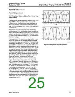
Note: Slew rate = 5.65 V/ms; trise = tfall = 23 ms; pwidth = 2 ms;
period = 50 ms.
205 x VCC/RICM (kΩ) = ITH (mA)
Additionally, a filter capacitor across RICM will set the
time constant of the detector. No hysteresis is associ-
ated with this detector. The RC filter at ICM gives
immunity to longitudinal currents.
Figure 8. Ringing Waveform Crest Factor = 1.6
80
60
Also in the ground start mode, the fixed loop current
threshold associated with the NSTAT detector output is
internally adjusted to account for common-mode cur-
rent detection in ground start mode (as opposed to dif-
ferential current in loop start mode); therefore, maintain
the detector at 10 mA. Thus, NSTAT may also be used
for loop closure detion in ground start. However, the
detector at NSTAT is not filtered against longitudinal
currents, which may or may not be an issue in short-
loop applications. Using NSTAT will also save compo-
nents at ICM.
40
20
0
–20
–40
–60
–80
0.00 0.04 0.08 0.12 0.16 0.20
0.02 0.06 0.10 0.14 0.18
TIME (s)
12-3347a (F)
Note: Slew rate = 10.83 V/ms; trise = tfall = 12 ms; pwidth = 13 ms;
period = 50 ms.
Power Ring
Figure 9. Ringing Waveform Crest Factor = 1.2
The device offers a ring mode, in which a balanced
power ring signal is provided to the tip/ring pair. During
the ring mode, a user-supplied low-voltage ring signal
is input to the device’s RINGIN input. This signal is
amplified to produce the balanced power ring signal.
The user may supply a sine wave input, PWM input, or
a square wave to produce sinusoidal or trapezoidal
ringing at tip and ring.
Voltage applied to the load may be increased by using
a filtered square wave input to produce a lower crest
factor trapezoidal power ring signal at tip and ring.
Various crest factors are shown for illustrative pur-
poses.
24
Agere Systems Inc.

 ZARLINK [ ZARLINK SEMICONDUCTOR INC ]