L9216B/H
Preliminary Data Sheet
September 2001
High-Voltage Ringing SLIC with Ground Start
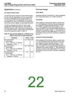
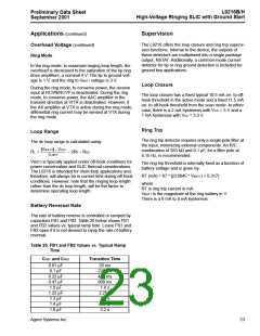
Supervision (continued)
Power Ring (continued)
Sine Wave Input Signal and Sine Wave Power Ring Signal Output (continued)
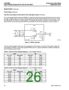
It is recommended that the input level at RINGIN be adjusted so that the power ring signal at tip and ring is just at
the edge or slightly clipping. This gives maximum power transfer with minimal distortion of the sine wave. The tip
side will saturate at a nominal 1 V above ground. The ring side will saturate at a nominal 3 V above battery. The
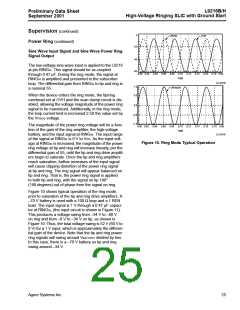
input circuit for a sine wave along with waveforms to illustrate the tip and ring saturation is shown in Figure 11.
L9216
PT
GND
+1
1 V
3 V
RINGIN
27.5x
0.47 µF
VTIP
INPUT
81 V
VRING
–1
VBAT
TR
100 kΩ
VBAT = –85 V
12-3532.I(F)
Figure 11. RINGIN Operation
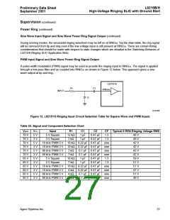
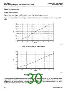
The point at which clipping of the power ring signal begins at tip and ring is a function of the battery voltage, the
input capacitor at RINGIN, and the input signal at RINGIN and Vcc. Typical characteristic conditions showing the
onset of clipping are given below.
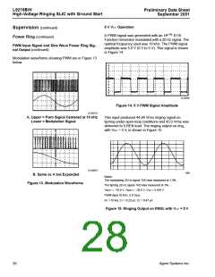
Table 21. Onset of Power Ringing Clipping VCC = 5 V, Cinput = 0.47 µF
Input
T/R
VBAT1 (V)
–70.15
–68.06
–66.00
–64.08
–62.04
–60.05
Vrms (mV)
891
Vrms (V)
46.88
45.11
Gain
52.62
52.58
52.45
52.30
52.23
52.36
858
833
43.69
42.57
41.21
39.11
814
789
747
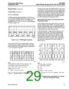
Table 22. Onset of Power Ringing Clipping VCC = 3.1 V, Cinput = 0.47 µF
Input T/R
VBAT1 (V)
–70.12
–68.07
–66.06
–64.01
–62.00
–60.00
Vrms (mV)
894
Vrms (V)
47.15
45.11
Gain
52.74
52.76
52.65
52.5
855
824
43.38
41.95
40.79
39.09
799
780
52.29
52.19
749
26
Agere Systems Inc.

 ZARLINK [ ZARLINK SEMICONDUCTOR INC ]