L9216B/H
Preliminary Data Sheet
September 2001
High-Voltage Ringing SLIC with Ground Start
During nonring modes, the PWM waveform may be left
on at RINGIN. Via the state table, the ring signal will be
removed from tip and ring even if the low-voltage input
is still present at RINGIN. There are certain timing con-
siderations that should be made with respect to state
changes which are detailed in the Switching Behavior
of L9215/6 Ringing SLIC Application Note.
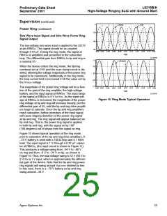
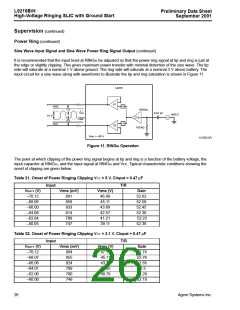
Supervision (continued)
Power Ring (continued)
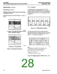
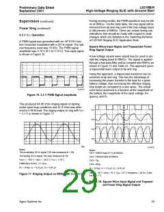
3.3 V VCC Operation
A PWM signal was generated with an HP 8116 Func-
tion Generator modulated with a 20 Hz signal. The opti-
mal frequency used was 10 kHz. The PWM signal
amplitude was 3.10 V (0 V to 3.10 V). This input signal
is shown in Figure 16.
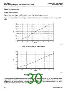
Square Wave Input Signal and Trapezoidal Power
Ring Signal Output
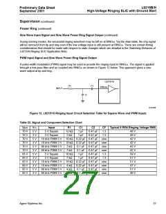
A low-voltage square wave signal may be used to pro-
vide the ringing input to RINGIN. The signal is applied
through a low-pass filter and ac-coupled into RINGIN as
shown in Figure 12 and Table 23. This approach gives
a trapezoidal wave output at tip and ring.
Using this approach, a trapezoidal waveform can be
achieved at tip and ring. This has the advantage of
increasing the power transfer to the load for a given
battery voltage, thus increasing the effective ringing
loop length as compared to a sine wave. The actual
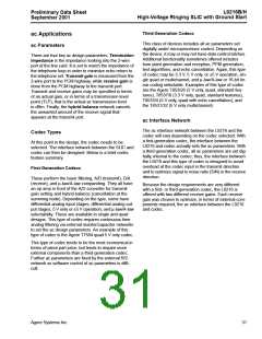
crest factor achieved is a function of the magnitude of
the battery, the magnitude of the input voltage, fre-
quency, and R1.
12-3571F
Figure 16. 3.3 V PWM Signal Amplitude
This produced 44.96 Vrms ringing signal on tip/ring
under open-loop conditions and 42.0 Vrms was deliv-
ered to 5 REN load. The ringing output on ring with VCC
= 3.1 V is shown in Figure 17.
CH1
CH2
CH3
CH4
1660
12-3572F
Notes:
Notes:
The modulating 20 Hz signal THD was measured at 1.3%.
CH1—CMOS Input (5 V) at RINGIN.
The tip/ring 20 Hz signal THD was measured at 1%.
VBAT1 = –70.6 V, VBAT2 = –26.5 V, VCC = 3.10 V.
PWM input 10 kHz, 3.1 Vp-p.
CH2—Filtered input at RINGIN.
CH3—Tip.
CH4—Ring.
R1 = 10 kΩ, C1 = 0.22 µF, C2 = 0.47 µF.
R1 = 14 kΩ, C1 = 1.0 µF, C2 = 0.47 µF.
VBAT1 = –70 V, Vrms = 51 V, Vp-p = 67 V, frequency = 20 Hz, Crest
Factor = 1.3.
Figure 17. Ringing Output on RING, with VCC = 3.1 V
Figure 18. Square Wave Input Signal and Trapezoi-
dal Power Ring Signal Output
Agere Systems Inc.
29

 ZARLINK [ ZARLINK SEMICONDUCTOR INC ]