L9216B/H
Preliminary Data Sheet
September 2001
High-Voltage Ringing SLIC with Ground Start
Supervision (continued)
Power Ring (continued)
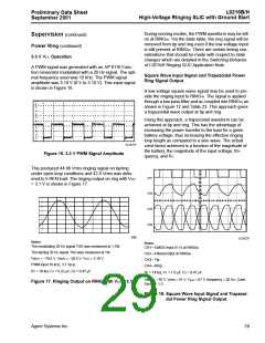
0
VRING
VTIP
–20
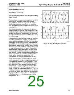
Sine Wave Input Signal and Sine Wave Power Ring
Signal Output
–40
–60
The low-voltage sine wave input is applied to the L9216
at pin RINGIN. This signal should be ac-coupled
through 0.47 µF. During the ring mode, the signal at
RINGIN is amplified and presented to the subscriber
loop. The differential gain from RINGIN to tip and ring is
a nominal 55.
0.60 0.62
0.64
0.66
0.68
0.70
0.72
0.74
0.76
0.78 0.80
TIME
12-3573F
1.0
VRINGIN
0.5
When the device enters the ring mode, the tip/ring
overhead set at OVH and the scan clamp circuit is dis-
abled, allowing the voltage magnitude of the power ring
signal to be maximized. Additionally, in the ring mode,
the loop current limit is increased 2.5X the value set by
the VPROG voltage.
0.0
–0.5
–1.0
The magnitude of the power ring voltage will be a func-
tion of the gain of the ring amplifier, the high-voltage
battery, and the input signal at RINGIN. The input range
of the signal at RINGIN is 0 V to Vcc. As the input volt-
age at RINGIN is increased, the magnitude of the power
ring voltage at tip and ring will increase linearly, per the
differential gain of 55, until the tip and ring drive amplifi-
ers begin to saturate. Once the tip and ring amplifiers
reach saturation, further increases of the input signal
will cause clipping distortion of the power ring signal
at tip and ring. The ring signal will appear balanced on
tip and ring. That is, the power ring signal is applied
to both tip and ring, with the signal on tip 180°
0.60 0.62
0.64
0.66
0.68
0.70
TIME
0.72
0.74
0.76
0.78 0.80
12-3574F
Figure 10. Ring Mode Typical Operation
(180 degrees) out of phase from the signal on ring.
Figure 10 shows typical operation of the ring mode,
prior to saturation of the tip and ring drive amplifiers. A
–70 V battery is used with a 100 Ω loop and a 1 REN
load. The input signal is 1 V through a 0.47 µF capaci-
tor at RINGIN, (the input circuit is shown in Figure 11).
This produces a voltage swing from –34 V to –60 V
on ring and from –8 V to –34 V on tip, as shown in
Figure 10. Thus, the total voltage swing is 52 V (60 V to
8 V) for a 1 V input, which is approximately the differen-
tial gain of the device. Note that the tip and ring power
ring signals will swing around VBATTERY divided by two.
In this case, there is a –70 V battery so tip and ring
swing around –34 V.
Agere Systems Inc.
25

 ZARLINK [ ZARLINK SEMICONDUCTOR INC ]