R
QPRO XQ4000E/EX QML High-Reliability FPGAs
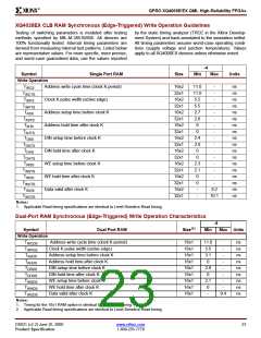
XQ4028EX CLB RAM Asynchronous (Level-Sensitive) Write and Read Operation Guidelines
Testing of switching parameters is modeled after testing
methods specified by MIL-M-38510/605. All devices are
100% functionally tested. Internal timing parameters are
derived from measuring internal test patterns. Listed below
are representative values. For more specific, more precise,
and worst-case guaranteed data, use the values reported
by the static timing analyzer (TRCE in the Xilinx Develop-
ment System) and back-annotated to the simulation netlist.
All timing parameters assume worst-case operating condi-
tions (supply voltage and junction temperature). Values
apply to all XQ4000EX devices unless otherwise noted.
-4
Symbol
Single Port RAM
Size
Min
Max
Units
Write Operation
T
Address write cycle time
16x2
32x1
16x2
32x1
16x2
32x1
16x2
32x1
16x2
32x1
16x2
32x1
10.6
10.6
5.3
5.3
2.8
2.8
1.7
1.7
1.1
1.1
6.6
6.6
-
-
-
-
-
-
-
-
-
-
-
-
ns
ns
ns
ns
ns
ns
ns
ns
ns
ns
ns
ns
WC
T
WCT
T
Write Enable pulse width (High)
Address setup time before WE
Address hold time after end of WE
DIN setup time before end of WE
DIN hold time after end of WE
WP
T
WPT
T
AS
T
AST
T
AH
T
AHT
T
DS
T
T
DST
T
DH
DHT
Read Operation
T
Address read cycle time
16x2
32x1
16x2
32x1
4.5
6.5
-
-
ns
ns
ns
ns
RC
T
-
RCT
T
Data valid after address change (no Write Enable)
2.2
3.8
ILO
T
-
IHO
Read Operation, Clocking Data into Flip-Flop
Address setup time before clock K
T
16x2
32x1
1.5
3.2
-
-
ns
ns
ICK
T
IHCK
Read During Write
T
Data valid after WE goes active (DIN stable before WE)
16x2
32x1
16x2
32x1
-
-
-
-
6.5
7.4
7.7
8.2
ns
ns
ns
ns
WO
T
WOT
T
Data valid after DIN (DIN changes during WE)
DO
T
DOT
Read During Write, Clocking Data into Flip-Flop
T
WE setup time before clock K
16x2
32x1
16x2
32x1
7.1
9.2
5.9
8.4
-
-
-
-
ns
ns
ns
ns
WCK
T
WCKT
T
Data setup time before clock K
DCK
T
DOCK
Notes:
1. Timing for the 16x1 RAM option is identical to 16x2 RAM timing.
DS021 (v2.2) June 25, 2000
Product Specification
www.xilinx.com
1-800-255-7778
25

 XILINX [ XILINX, INC ]