R
QPRO XQ4000E/EX QML High-Reliability FPGAs
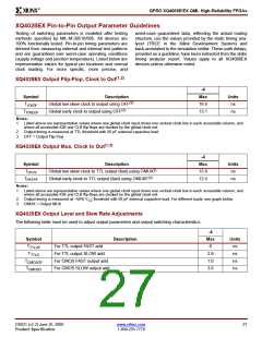
XQ4028EX Pin-to-Pin Output Parameter Guidelines
Testing of switching parameters is modeled after testing
methods specified by MIL-M-38510/605. All devices are
100% functionally tested. Pin-to-pin timing parameters are
derived from measuring external and internal test patterns
and are guaranteed over worst-case operating conditions
(supply voltage and junction temperature). Listed below are
representative values for typical pin locations and normal
clock loading. For more specific, more precise, and
worst-case guaranteed data, reflecting the actual routing
structure, use the values provided by the static timing ana-
lyzer (TRCE in the Xilinx Development System) and
back-annotated to the simulation netlist. These path delays,
provided as a guideline, have been extracted from the static
timing analyzer report. Values apply to all XQ4000EX
devices unless otherwise noted.
XQ4028EX Output Flip-Flop, Clock to Out(1,2)
-4
Symbol
Description
Max
16.6
13.1
Units
ns
(3)
T
Global low skew clock to output using OFF
ICKOF
(3)
T
Global early clock to output using OFF
ns
ICKEOF
Notes:
1. Listed above are representative values where one global clock input drives one vertical clock line in each accessible column, and
where all accessible IOB and CLB flip-flops are clocked by the global clock net.
2. Output timing is measured at TTL threshold with 50 pF external capacitive load.
3. OFF = Output Flip-Flop
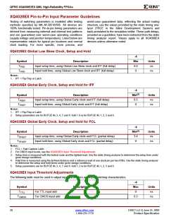
XQ4028EX Output Mux, Clock to Out(1,2)
-4
Symbol
Description
Max
15.9
12.4
Units
ns
3)
T
Global low skew clock to TTL output (fast) using OMUX
PFPF
(3)
T
Global early clock to TTL output (fast) using OMUXF
ns
PEFPF
Notes:
1. Listed above are representative values where one global clock input drives one vertical clock line in each accessible column, and
where all accessible IOB and CLB flip-flops are clocked by the global clock net.
2. Output timing is measured at ~50% V threshold with 50 pF external capacitive load. For different loads, see graph below.
CC
3. OMUX = Output MUX
XQ4028EX Output Level and Slew Rate Adjustments
The following table must be used to adjust output parameters and output switching characteristics.
-4
Symbol
Description
Max
0
Units
ns
T
For TTL output FAST add
For TTL output SLOW add
For CMOS FAST output add
For CMOS SLOW output add
TTLOF
T
2.9
1.0
3.6
ns
TTLO
T
ns
CMOSOF
T
ns
CMOSO
DS021 (v2.2) June 25, 2000
www.xilinx.com
27
Product Specification
1-800-255-7778

 XILINX [ XILINX, INC ]