R
Platform Flash In-System Programmable Configuration PROMS
TAP AC Parameters
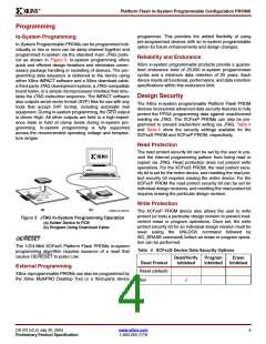
Table 8 shows the timing parameters for the TAP waveforms shown in Figure 6.
Table 8: Test Access Port Timing Parameters
Symbol
Parameter
Min
100
50
10
25
10
25
-
Max
Units
ns
T
T
T
T
T
T
T
TCK minimum clock period when V
= 2.5V or 3.3V
-
-
CKMIN1
CCJ
TCK minimum clock period, Bypass Mode, when V
= 2.5V or 3.3V
ns
CKMIN2
MSS
MSH
DIS
CCJ
TMS setup time when V
= 2.5V or 3.3V
-
ns
CCJ
TMS hold time when V
TDI setup time when V
= 2.5V or 3.3V
= 2.5V or 3.3V
-
ns
CCJ
CCJ
-
ns
TDI hold time when V
= 2.5V or 3.3V
-
ns
DIH
CCJ
TDO valid delay when V
= 2.5V or 3.3V
CCJ
30
ns
DOV
data value is held on the data outputs. While BUSY is High,
the PROM will continue driving the CLKOUT signal to the
FPGA, clocking the FPGA’s configuration logic. When the
FPGA deasserts BUSY, indicating that it is ready to receive
additional configuration data, the PROM will begin driving
new data onto the configuration interface.
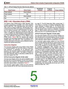
Additional Features for the XCFxxP
Internal Oscillator
The 8/16/32 Mbit XCFxxP Platform Flash PROMs include
an optional internal oscillator which can be used to drive the
CLKOUT and DATA pins on FPGA configuration interface.
The internal oscillator can be enabled during device pro-
gramming, and can be set to either the default frequency or
to a slower frequency (AC Characteristics Over Operat-
ing Conditions When Cascading).
Decompression
The 8/16/32 Mbit XCFxxP Platform Flash PROMs include a
built-in data decompressor compatible with Xilinx advanced
compression technology. Compressed Platform Flash
PROM files are created from the target FPGA bitstream(s)
using the iMPACT software. Only Slave Serial and Slave
SelectMAP (parallel) configuration modes are supported for
FPGA configuration when using a XCFxxP PROM pro-
grammed with a compressed bitstream. Compression rates
will vary depending on several factors, including the target
device family and the target design contents.
CLKOUT
The 8/16/32 Mbit XCFxxP Platform Flash PROMs include
the programmable option to enable the CLKOUT signal
which allows the PROM to provide a source synchronous
clock aligned to the data on the configuration interface. The
CLKOUT signal is derived from one of two clock sources:
the CLK input pin or the internal oscillator. The input clock
source is selected during the PROM programming
sequence. Output data is available on the rising edge of
CLKOUT.
The decompression option is enabled during the PROM
programming sequence. The PROM decompresses the
stored data before driving both clock and data onto the
FPGA's configuration interface. If Decompression is
enabled, then the Platform Flash clock output pin (CLK-
OUT) must be used as the clock signal for the configuration
interface, driving the target FPGA's configuration clock input
pin (CCLK). Either the PROM's CLK input pin or the internal
oscillator must be selected as the source for CLKOUT. Any
target FPGA connected to the PROM must operate as slave
in the configuration chain, with the configuration mode set to
Slave Serial mode or Slave SelectMap (parallel) mode.
The CLKOUT signal is enabled during programming, and is
active when CE is Low and OE/RESET is High. When dis-
abled, the CLKOUT pin is put into a high-impedance state
and should be pulled High externally to provide a known
state.
When cascading Platform Flash PROMs with CLKOUT
enabled, after completing it's data transfer, the first PROM
disables CLKOUT and releases the CEO pin enabling the
next PROM in the PROM chain. The next PROM will begin
driving the CLKOUT signal once that PROM is enabled and
data is available for transfer.
When decompression is enabled, the CLKOUT signal
becomes a controlled clock output with a reduced maximum
frequency and remains Low when decompressed data is
not ready.
During high-speed parallel configuration without compres-
sion, the FPGA drives the BUSY signal on the configuration
interface. When BUSY is asserted High, the PROMs inter-
nal address counter stops incrementing, and the current
The BUSY input is automatically disabled when decompres-
sion is enabled.
DS123 (v2.4) July 20, 2004
Preliminary Product Specification
www.xilinx.com
1-800-255-7778
8

 XILINX [ XILINX, INC ]