R
Platform Flash In-System Programmable Configuration PROMS
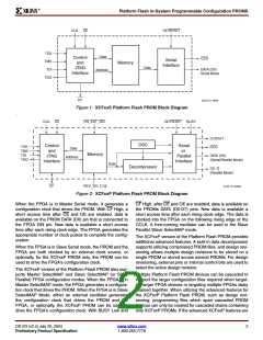
Table 6: Platform Flash PROM Boundary Scan Instructions
XCFxxS IR[7:0] XCFxxP IR[15:0]
Boundary-Scan Command
Required Instructions
BYPASS
(hex)
(hex)
Instruction Description
Enables BYPASS
FF
01
00
FFFF
0001
0000
Enables boundary-scan SAMPLE/PRELOAD operation
Enables boundary-scan EXTEST operation
SAMPLE/PRELOAD
EXTEST
Optional Instructions
CLAMP
Enables boundary-scan CLAMP operation
FA
FC
00FA
00FC
Places all outputs in high-impedance state
simultaneously
HIGHZ
Enables shifting out 32-bit IDCODE
IDCODE
FE
FD
00FE
00FD
Enables shifting out 32-bit USERCODE
USERCODE
PlatformFlashPROMSpecific
Instructions
Initiates FPGA configuration by pulsing CF pin Low
once. (For the XCFxxP this command also resets the
selected design revision based on either the external
REV_SEL[1:0] pins or on the internal design revision
selection bits.)(1)
CONFIG
EE
00EE
Notes:
1. For more information see Initiating FPGA Configuration.
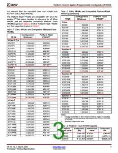
IR[7:5]
IR[4]
IR[3]
Security
IR[2]
IR[1:0]
TDI →
→ TDO
Reserved
ISC Status
0
0 1
Figure 4: XCFxxS Instruction Capture Values Loaded into IR as part of an Instruction Scan Sequence
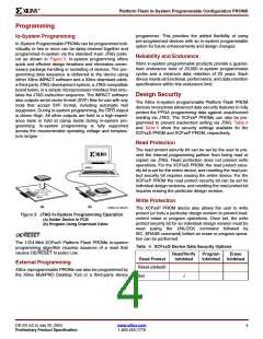
IR[15:9]
IR[8:7]
IR[6:5]
ER/PROG ER/PROG
Error Status
IR[4]
IR[3]
IR[2]
IR[1:0]
TDI →
→ TDO
Reserved
ISC Error
ISC Status
DONE
0 1
Figure 5: XCFxxP Instruction Capture Values Loaded into IR as part of an Instruction Scan Sequence
Boundary Scan Register
The boundary-scan register is used to control and observe
the state of the device pins during the EXTEST, SAM-
PLE/PRELOAD, and CLAMP instructions. Each output pin
on the Platform Flash PROM has two register stages which
contribute to the boundary-scan register, while each input
pin has only one register stage. The bidirectional pins have
a total of three register stages which contribute to the
boundary-scan register. For each output pin, the register
stage nearest to TDI controls and observes the output state,
and the second stage closest to TDO controls and observes
the High-Z enable state of the output pin. For each input pin,
a single register stage controls and observes the input state
of the pin. The bidirectional pin combines the three bits, the
input stage bit is first, followed by the output stage bit and
finally the output enable stage bit. The output enable stage
bit is closest to TDO.
See the XCFxxS/XCFxxP Pin Names and Descriptions
Tables in the Pinouts and Pin Descriptions section for the
boundary-scan bit order for all connected device pins, or
see the appropriate BSDL file for the complete bound-
ary-scan bit order description under the "attribute
BOUNDARY_REGISTER" section in the BSDL file. The bit
assigned to boundary-scan cell "0" is the LSB in the bound-
ary-scan register, and is the register bit closest to TDO.
DS123 (v2.4) July 20, 2004
Preliminary Product Specification
www.xilinx.com
1-800-255-7778
6

 XILINX [ XILINX, INC ]