R
Platform Flash In-System Programmable Configuration PROMS
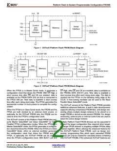
Programming
programmer. This provides the added flexibility of using
pre-programmed devices with an in-system programmable
option for future enhancements and design changes.
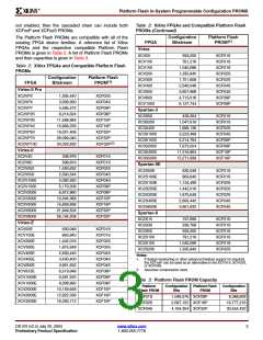
In-System Programming
In-System Programmable PROMs can be programmed indi-
vidually, or two or more can be daisy-chained together and
programmed in-system via the standard 4-pin JTAG proto-
col as shown in Figure 3. In-system programming offers
quick and efficient design iterations and eliminates unnec-
essary package handling or socketing of devices. The pro-
gramming data sequence is delivered to the device using
either Xilinx iMPACT software and a Xilinx download cable,
a third-party JTAG development system, a JTAG-compatible
board tester, or a simple microprocessor interface that emu-
lates the JTAG instruction sequence. The iMPACT software
also outputs serial vector format (SVF) files for use with any
tools that accept SVF format, including automatic test
equipment. During in-system programming, the CEO output
is driven High. All other outputs are held in a high-imped-
ance state or held at clamp levels during in-system pro-
gramming. In-system programming is fully supported
across the recommended operating voltage and tempera-
ture ranges.
Reliability and Endurance
Xilinx in-system programmable products provide a guaran-
teed endurance level of 20,000 in-system program/erase
cycles and a minimum data retention of 20 years. Each
device meets all functional, performance, and data retention
specifications within this endurance limit.
Design Security
The Xilinx in-system programmable Platform Flash PROM
devices incorporate advanced data security features to fully
protect the FPGA programming data against unauthorized
reading via JTAG. The XCFxxP PROMs can also be pro-
grammed to prevent inadvertent writing via JTAG. Table 4
and Table 5 show the security settings available for the
XCFxxS PROM and XCFxxP PROM, respectively.
Read Protection
The read protect security bit can be set by the user to pre-
vent the internal programming pattern from being read or
copied via JTAG. Read protection does not prevent write
operations. For the XCFxxS PROM, the read protect secu-
rity bit is set for the entire device, and resetting the read pro-
tect security bit requires erasing the entire device. For the
XCFxxP PROM the read protect security bit can be set for
individual design revisions, and resetting the read protect bit
requires erasing the particular design revision.
Write Protection
(a)
(b)
DS026_02_082703
The XCFxxP PROM device also allows the user to write
protect (or lock) a particular design revision to prevent inad-
vertent erase or program operations. Once set, the write
protect security bit for an individual design revision must be
reset (using the UNLOCK command followed by
ISC_ERASE command) before an erase or program opera-
tion can be performed.
Figure 3: JTAG In-System Programming Operation
(a) Solder Device to PCB
(b) Program Using Download Cable
OE/RESET
The 1/2/4 Mbit XCFxxS Platform Flash PROMs in-system
programming algorithm requires issuance of a reset that
causes OE/RESET to pulse Low.
Table 4: XCFxxS Device Data Security Options
Read/Verify
Inhibited
Program
Inhibited
Erase
Inhibited
Read Protect
Reset (default)
Set
External Programming
Xilinx reprogrammable PROMs can also be programmed by
the Xilinx MultiPRO Desktop Tool or a third-party device
√
DS123 (v2.4) July 20, 2004
Preliminary Product Specification
www.xilinx.com
1-800-255-7778
4

 XILINX [ XILINX, INC ]