R
Platform Flash In-System Programmable Configuration PROMS
USERCODE Register
Identification Registers
The USERCODE instruction gives access to a 32-bit user
programmable scratch pad typically used to supply informa-
IDCODE Register
The IDCODE is a fixed, vendor-assigned value that is used
to electrically identify the manufacturer and type of the
device being addressed. The IDCODE register is 32 bits
wide. The IDCODE register can be shifted out for examina-
tion by using the IDCODE instruction. The IDCODE is avail-
able to any other system component via JTAG. Table 7 lists
the IDCODE register values for the Platform Flash PROMs.
tion about the device's programmed contents. By using the
USERCODE instruction, a user-programmable identifica-
tion code can be shifted out for examination. This code is
loaded into the USERCODE register during programming of
the Platform Flash PROM. If the device is blank or was not
loaded during programming, the USERCODE register con-
tains FFFFFFFFh.
The IDCODE register has the following binary format:
vvvv:ffff:ffff:aaaa:aaaa:cccc:cccc:ccc1
where
Customer Code Register
For the XCFxxP Platform Flash PROM, in addition to the
USERCODE, a unique 32-byte Customer Code can be
assigned to each design revision enabled for the PROM.
The Customer Code is set during programming, and is typ-
ically used to supply information about the design revision
contents. A private JTAG instruction is required to read the
Customer Code. If the PROM is blank, or the Customer
Code for the selected design revision was not loaded during
programming, or if the particular design revision is erased,
the Customer Code will contain all ones.
v = the die version number
f = the PROM family code
a = the specific Platform Flash PROM product ID
c = the Xilinx manufacture's ID
The LSB of the IDCODE register is always read as logic "1"
as defined by IEEE Std. 1149.1.
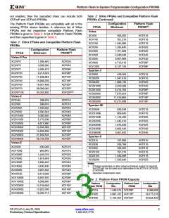
Table 7: IDCODES Assigned to Platform Flash PROMs
(1)
Device
XCF01S
XCF02S
XCF04S
XCF08P
XCF16P
XCF32P
IDCODE (hex)
05044093
05045093
05046093
05057093
05058093
05059093
Platform Flash PROM TAP
Characteristics
The Platform Flash PROM family performs both in-system
programming and IEEE 1149.1 boundary-scan (JTAG) test-
ing via a single 4-wire Test Access Port (TAP). This simpli-
fies system designs and allows standard Automatic Test
Equipment to perform both functions. The AC characteris-
tics of the Platform Flash PROM TAP are described as fol-
lows.
Notes:
TAP Timing
1. The first four bits indicate the die version number, and may
vary.
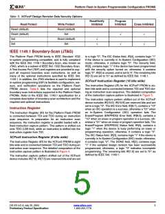
Figure 6 shows the timing relationships of the TAP signals.
These TAP timing characteristics are identical for both
boundary-scan and ISP operations.
T
CKMIN
TCK
TMS
T
T
MSS
MSH
T
T
DIH
DIS
TDI
T
DOV
TDO
DS026_04_020300
Figure 6: Test Access Port Timing
DS123 (v2.4) July 20, 2004
www.xilinx.com
7
Preliminary Product Specification
1-800-255-7778

 XILINX [ XILINX, INC ]