Artix-7 FPGAs Data Sheet: DC and AC Switching Characteristics
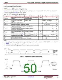
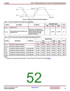
X-Ref Target - Figure 5
TRCLK
80%
20%
TFCLK
Figure 5: Reference Clock Timing Parameters
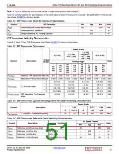
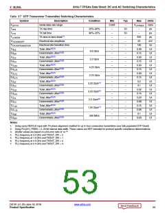
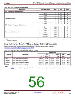
Table 55: GTP Transceiver PLL/Lock Time Adaptation
ds181_03_062811
All Speed Grades
Symbol
Description
Initial PLL lock
Conditions
Units
Min
Typ
Max
TLOCK
–
–
1
ms
After the PLL is locked to the
reference clock, this is the time it
takes to lock the clock data
recovery (CDR) to the data
present at the input.
Clock recovery phase acquisition and
adaptation time.
TDLOCK
–
50,000
2.3 x10⁶
UI
(1)
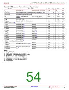
Table 56: GTP Transceiver User Clock Switching Characteristics
Speed Grade
Symbol
Description
Conditions
1.0V
0.95V
-1LI
0.9V
Units
-3
-2/-2LE
412.500
412.500
412.500
412.500
412.500
412.500
-1
-2LE
FTXOUT
TXOUTCLK maximum frequency
412.500
412.500
412.500
412.500
412.500
412.500
234.375
234.375
234.375
234.375
234.375
234.375
234.375
234.375
234.375
234.375
234.375
234.375
234.375
234.375
234.375
234.375
234.375
234.375
MHz
MHz
MHz
MHz
MHz
MHz
FRXOUT RXOUTCLK maximum frequency
FTXIN
TXUSRCLK maximum frequency
RXUSRCLK maximum frequency
16-bit data path
16-bit data path
FRXIN
FTXIN2
FRXIN2
TXUSRCLK2 maximum frequency 16-bit data path
RXUSRCLK2 maximum frequency 16-bit data path
Notes:
1. Clocking must be implemented as described in 7 Series FPGAs GTP Transceiver User Guide (UG482).
DS181 (v1.25) June 18, 2018
www.xilinx.com
Product Specification
52

 XILINX [ XILINX, INC ]