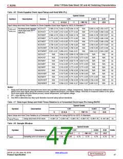
Artix-7 FPGAs Data Sheet: DC and AC Switching Characteristics
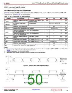
Note: In Figure 4, differential peak-to-peak voltage = single-ended peak-to-peak voltage x 2.
Table 51 summarizes the DC specifications of the clock input of the GTP transceiver. Consult 7 Series FPGAs GTP Transceiver
User Guide (UG482) for further details.
Table 51: GTP Transceiver Clock DC Input Level Specification
Symbol
VIDIFF
DC Parameter
Differential peak-to-peak input voltage
Min
350
–
Typ
–
Max
2000
–
Units
mV
Ω
RIN
Differential input resistance
100
100
CEXT
Required external AC coupling capacitor
–
–
nF
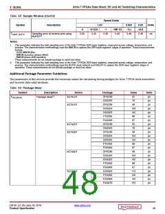
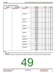
GTP Transceiver Switching Characteristics
Consult 7 Series FPGAs GTP Transceiver User Guide (UG482) for further information.
Table 52: GTP Transceiver Performance
Speed Grade
-1 (1.0V)
-2 (1.0V)
-2LE (1.0V)
-1LI (0.95V)
-1Q (1.0V)
-1M (1.0V)
-3 (1.0V)
-2LE (0.9V)
Output
Divider
Symbol
Description
Units
Package Type
FF
FB
SB
RB
RS
FF
FG
FB
FT
FG
FG
FT
CS
CP
FG
FF
FB
SB
FF
FT
FB
CS
SB
CP
FT
CS
CP
SB
CS
RB
CP
RS
FGTPMAX
Maximum GTP transceiver data rate
6.6
6.25
6.6
6.25
3.75
3.75
3.75
3.75
Gb/s
FGTPMIN
Minimum GTP transceiver data rate
1
0.500
0.500
0.500
0.500
0.500
0.500
0.500
0.500 Gb/s
3.2–6.6
3.2–6.6
3.2–3.75
3.2–3.75
1.6–3.2
Gb/s
Gb/s
Gb/s
Gb/s
GHz
2
1.6–3.3
0.8–1.65
0.5–0.825
1.6–3.3
1.6–3.3
0.8–1.65
0.5–0.825
1.6–3.3
1.6–3.2
0.8–1.6
0.5–0.8
1.6–3.3
FGTPRANGE
PLL line rate range
4
0.8–1.6
0.5–0.8
1.6–3.3
8
FGTPPLLRANGE GTP transceiver PLL frequency
range
Table 53: GTP Transceiver Dynamic Reconfiguration Port (DRP) Switching Characteristics
Speed Grade
Symbol
Description
1.0V
-2/-2LE
175
0.95V
-1LI
0.9V
-2LE
125
Units
-3
-1
FGTPDRPCLK
GTPDRPCLK maximum frequency
175
156
156
MHz
Table 54: GTP Transceiver Reference Clock Switching Characteristics
All Speed Grades
Symbol
Description
Conditions
Units
Min
60
–
Typ
–
Max
660
–
FGCLK
TRCLK
TFCLK
TDCREF
Reference clock frequency range
Reference clock rise time
Reference clock fall time
MHz
ps
20ꢀ – 80ꢀ
200
200
–
80ꢀ – 20ꢀ
–
–
ps
Reference clock duty cycle
Transceiver PLL only
40
60
ꢀ
DS181 (v1.25) June 18, 2018
www.xilinx.com
Product Specification
51

 XILINX [ XILINX, INC ]