Artix-7 FPGAs Data Sheet: DC and AC Switching Characteristics
GTP Transceiver Specifications
GTP Transceiver DC Input and Output Levels
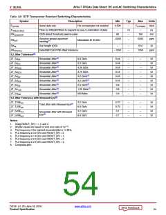
Table 50 summarizes the DC output specifications of the GTP transceivers in Artix-7 FPGAs. Consult 7 Series FPGAs GTP
Transceiver User Guide (UG482) for further details.
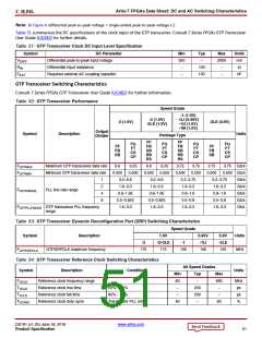
Table 50: GTP Transceiver DC Specifications
Symbol
DC Parameter
Conditions
Min
Typ
Max
Units
Differential peak-to-peak output Transmitter output swing is set to
1000
–
–
mV
DVPPOUT
voltage(1)
maximum setting
DC common mode output
voltage
Equation based
VMGTAVTT – DVPPOUT/4
mV
VCMOUTDC
ROUT
Differential output resistance
–
100
–
Ω
mV
ps
VCMOUTAC
Common mode output voltage: AC coupled
1/2 VMGTAVTT
–
Transmitter output pair (TXP and TXN) intra-pair skew
(FF, FB, SB packages)
–
–
10
12
TOSKEW
Transmitter output pair (TXP and TXN) intra-pair skew
(FG, FT, CS, CP packages)
–
ps
Differential peak-to-peak input External AC coupled
voltage
150
–
2000
mV
DVPPIN
VIN
Single-ended input voltage(2)
Common mode input voltage
Differential input resistance
DC coupled VMGTAVTT = 1.2V
DC coupled VMGTAVTT = 1.2V
–200
–
2/3 VMGTAVTT
100
VMGTAVTT mV
VCMIN
RIN
–
–
–
–
–
–
mV
Ω
CEXT
Recommended external AC coupling capacitor(3)
100
nF
Notes:
1. The output swing and preemphasis levels are programmable using the attributes discussed in 7 Series FPGAs GTP Transceiver User Guide
(UG482) and can result in values lower than reported in this table.
2. Voltage measured at the pin referenced to ground.
3. Other values can be used as appropriate to conform to specific protocols and standards.
X-Ref Target - Figure 3
+V
0
P
N
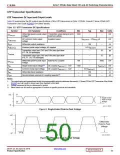
Single-Ended
Peak-to-Peak
Voltage
ds181_01_062014
Figure 3: Single-Ended Peak-to-Peak Voltage
X-Ref Target - Figure 4
+V
0
Differential
Peak-to-Peak
Voltage
P–N
–V
ds181_02_062014
Figure 4: Differential Peak-to-Peak Voltage
DS181 (v1.25) June 18, 2018
www.xilinx.com
Product Specification
50

 XILINX [ XILINX, INC ]