Virtex-6 FPGA Data Sheet: DC and Switching Characteristics
GTH Transceiver DC Input and Output Levels
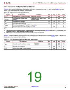
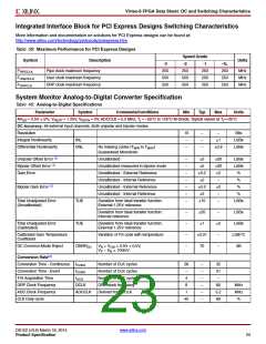
Table 30 summarizes the DC output specifications of the GTH transceivers in Virtex-6 FPGAs. Consult UG371:Virtex-6
FPGA GTH Transceivers User Guide for further details.
Table 30: GTH Transceiver DC Specifications
Symbol
DVPPIN
DC Parameter
Conditions
Min
175
800
Typ
–
Max
1200
1200
Units
mV
Differential peak-to-peak input voltage External AC coupled
Differential peak-to-peak output
voltage(1)
Transmitter output swing is set to
maximum setting
–
mV
DVPPOUT
RIN
Differential input resistance
Differential output resistance
80
80
–
100
100
2
120
120
–
Ω
Ω
ROUT
TOSKEW
CEXT
Transmitter output pair (TXP and TXN) intra-pair skew
Recommended external AC coupling capacitor(2)
ps
nF
–
100
–
Notes:
1. The output swing and preemphasis levels are programmable using the attributes discussed in UG371:Virtex-6 FPGA GTH Transceivers User
Guide and can result in values lower than reported in this table.
2. Other values can be used as appropriate to conform to specific protocols and standards.
Table 31 summarizes the DC specifications of the clock input of the GTH transceiver. Consult UG371:Virtex-6 FPGA GTH
Transceivers User Guide for further details.
Table 31: GTH Transceiver Clock DC Input Level Specification
Symbol
DC Parameter
Conditions
≤ 600 MHz
Min
500
600
80
Typ
–
Max
1600
1600
120
–
Units
mV
mV
Ω
VIDIFF
Differential peak-to-peak input voltage
> 600 MHz
–
RIN
Differential input resistance
100
100
CEXT
Required external AC coupling capacitor
–
nF
DS152 (v3.6) March 18, 2014
www.xilinx.com
Product Specification
19

 XILINX [ XILINX, INC ]