Virtex-6 FPGA Data Sheet: DC and Switching Characteristics
Integrated Interface Block for PCI Express Designs Switching Characteristics
More information and documentation on solutions for PCI Express designs can be found at:
http://www.xilinx.com/technology/protocols/pciexpress.htm
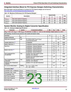
Table 39: Maximum Performance for PCI Express Designs
Speed Grade
Symbol
Description
Units
-3
-2
-1
-1L
250
250
250
FPIPECLK
FUSERCLK
FDRPCLK
Pipe clock maximum frequency
250
500
250
250
500
250
250
250
250
MHz
MHz
MHz
User clock maximum frequency
DRP clock maximum frequency
System Monitor Analog-to-Digital Converter Specification
Table 40: Analog-to-Digital Specifications
Parameter
Symbol
Comments/Conditions
Min
Typ
Max
Units
AVDD = 2.5V 5%, VREFP = 1.25V, VREFN = 0V, ADCCLK = 5.2 MHz, Tj = –55°C to 125°C M-Grade, Typical values at Tj=+35°C
DC Accuracy: All external input channels. Both unipolar and bipolar modes.
Resolution
10
–
–
–
–
–
Bits
Integral Nonlinearity
Differential Nonlinearity
INL
1
LSBs
LSBs
DNL
No missing codes (TMIN to TMAX
)
–
0.9
Guaranteed Monotonic
Unipolar Offset Error (1)
Bipolar Offset Error (1)
Gain Error
Uncalibrated
–
–
–
–
–
–
–
2
30
30
2
LSBs
LSBs
%
Uncalibrated measured in bipolar mode
Uncalibrated - External Reference
Uncalibrated - Internal Reference
Uncalibrated - External Reference
Uncalibrated - Internal Reference
2
0.2
2
–
%
Bipolar Gain Error (1)
0.2
2
2
%
–
%
Total Unadjusted Error
(Uncalibrated)
TUE
Deviation from ideal transfer function.
External 1.25V reference
10
–
LSBs
Deviation from ideal transfer function.
Internal reference
–
–
–
–
20
1
–
2
–
–
LSBs
LSBs
LSB/°C
dB
Total Unadjusted Error
(Calibrated)
TUE
Deviation from ideal transfer function.
External 1.25V reference
Calibrated Gain Temperature
Coefficient
Variation of FS code with temperature
0.01
70
DC Common-Mode Reject
CMRRDC
VN = VCM = 0.5V 0.5V,
VP – VN = 100mV
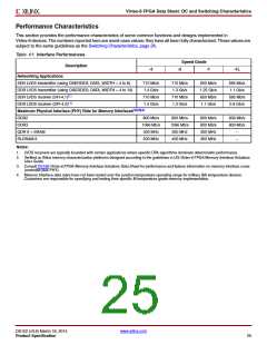
Conversion Rate(2)
Conversion Time - Continuous tCONV
Number of CLK cycles
Number of CLK cycles
Number of CLK cycles
DRP clock frequency
Derived from DCLK
26
–
–
–
–
–
–
–
32
21
–
Conversion Time - Event
T/H Acquisition Time
DRP Clock Frequency
ADC Clock Frequency
CLK Duty cycle
tCONV
tACQ
4
DCLK
ADCCLK
8
80
5.2
60
MHz
MHz
%
1
40
DS152 (v3.6) March 18, 2014
www.xilinx.com
Product Specification
23

 XILINX [ XILINX, INC ]