Spartan-3E FPGA Family: Functional Description
Start-Up
At the end of configuration, the FPGA automatically pulses
the Global Set/Reset (GSR) signal, placing all flip-flops in a
known state. After configuration completes, the FPGA
switches over to the user application loaded into the FPGA.
The sequence and timing of how the FPGA switches over is
programmable as is the clock source controlling the
sequence.
The function of the dual-purpose I/O pins, such as M[2:0],
VS[2:0], HSWAP, and A[23:0], also changes when the
DONE pin goes High. When DONE is High, these pins
become user I/Os. Like all user-I/O pins, GTS controls when
the dual-purpose pins can drive out.
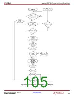
The relative timing of configuration events is programmed
via the Bitstream Generator (BitGen) options in the Xilinx
development software. For example, the GTS and GWE
events can be programmed to wait for all the DONE pins to
High on all the devices in a multiple-FPGA daisy-chain,
forcing the FPGAs to start synchronously. Similarly, the
start-up sequence can be paused at any stage, waiting for
selected DCMs to lock to their respective input clock
signals. See also Stabilizing DCM Clocks Before User
Mode.
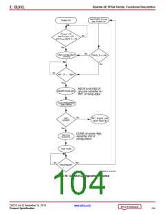
The default start-up sequence appears in Figure 68, where
the Global Three-State signal (GTS) is released one clock
cycle after DONE goes High. This sequence allows the
DONE signal to enable or disable any external logic used
during configuration before the user application in the FPGA
starts driving output signals. One clock cycle later, the
Global Write Enable (GWE) signal is released. This allows
signals to propagate within the FPGA before any clocked
storage elements such as flip-flops and block ROM are
enabled.
By default, the start-up sequence is synchronized to CCLK.
Alternatively, the start-up sequence can be synchronized to
a user-specified clock from within the FPGA application
using the STARTUP_SPARTAN3E library primitive and by
setting the StartupClk bitstream generator option. The
FPGA application can optionally assert the GSR and GTS
signalsviatheSTARTUP_SPARTAN3Eprimitive. ForJTAG
configuration, the start-up sequence can be synchronized
to the TCK clock input.
X-Ref Target - Figure 68
Default Cycles
Start-Up Clock
Phase
0
1
2
3
4
5
6 7
DONE
GTS
GWE
Sync-to-DONE
Start-Up Clock
Phase
0
1
2
3
4
5
6 7
DONE High
DONE
GTS
GWE
DS312-2_60_022305
Figure 68: Default Start-Up Sequence
DS312 (v4.2) December 14, 2018
www.xilinx.com
Product Specification
106

 XILINX [ XILINX, INC ]