Spartan-3E FPGA Family: Functional Description
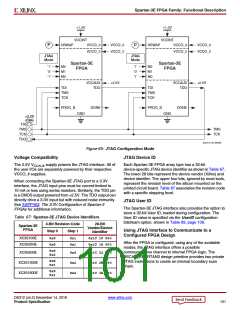
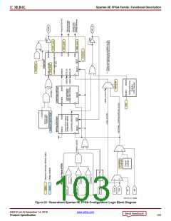
X-Ref Target - Figure 65
+1.2V
+1.2V
VCCINT
VCCINT
P
HSWAP
VCCO_0
VCCO_0
VCCO_2
HSWAP
VCCO_0
VCCO_0
VCCO_2
P
VCCO_2
VCCO_2
JTAG
Mode
JTAG
Mode
Spartan-3E
Spartan-3E
FPGA
‘1’
‘0’
‘1’
M2
M1
M0
‘1’
‘0’
‘1’
M2
M1
M0
FPGA
VCCAUX
+2.5V
VCCAUX
TDO
+2.5V
TDI
TDO
TDI
TMS
TCK
TMS
TCK
PROG_B
DONE
PROG_B
DONE
GND
GND
+2.5V
JTAG
TDI
TMS
TCK
TDO
TMS
TCK
DS312-2_56_082009
Figure 65: JTAG Configuration Mode
Voltage Compatibility
JTAG Device ID
The 2.5V V
supply powers the JTAG interface. All of
Each Spartan-3E FPGA array type has a 32-bit
CCAUX
the user I/Os are separately powered by their respective
VCCO_# supplies.
device-specific JTAG device identifier as shown in Table 67.
The lower 28 bits represent the device vendor (Xilinx) and
device identifer. The upper four bits, ignored by most tools,
represent the revision level of the silicon mounted on the
printed circuit board. Table 67 associates the revision code
with a specific stepping level.
When connecting the Spartan-3E JTAG port to a 3.3V
interface, the JTAG input pins must be current-limited to
10 mA or less using series resistors. Similarly, the TDO pin
is a CMOS output powered from +2.5V. The TDO output can
directly drive a 3.3V input but with reduced noise immunity.
See XAPP453: The 3.3V Configuration of Spartan-3
FPGAs for additional information.
JTAG User ID
The Spartan-3E JTAG interface also provides the option to
store a 32-bit User ID, loaded during configuration. The
User ID value is specified via the UserID configuration
bitstream option, shown in Table 69, page 108.
Table 67: Spartan-3E JTAG Device Identifiers
4-Bit Revision Code
28-Bit
Vendor/Device
Identifier
Spartan-3E
FPGA
Using JTAG Interface to Communicate to a
Configured FPGA Design
Step 0
Step 1
XC3S100E
XC3S250E
0x0
0x0
0x1
0x1
0x1C 10 093
0x1C 1A 093
After the FPGA is configured, using any of the available
modes, the JTAG interface offers a possible
communications channel to internal FPGA logic. The
BSCAN_SPARTAN3 design primitive provides two private
JTAG instructions to create an internal boundary scan
chain.
0x0
0x2
XC3S500E
XC3S1200E
XC3S1600E
0x4
0x2
0x2
0x1C 22 093
0x1C 2E 093
0x1C 3A 093
0x0
0x1
0x0
0x1
DS312 (v4.2) December 14, 2018
www.xilinx.com
Product Specification
101

 XILINX [ XILINX, INC ]