Spartan-3E FPGA Family: Functional Description
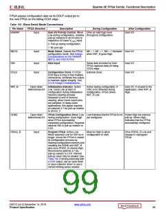
X-Ref Target - Figure 62
D[7:0]
CCLK
+1.2V
+1.2V
VCCINT
VCCINT
P
HSWAP
VCCO_0
VCCO_0
VCCO_1
P
HSWAP
VCCO_0
VCCO_0
VCCO_1
VCCO_1
LDC0
LDC1
HDC
VCCO_1
LDC0
LDC1
HDC
Slave
Parallel
Mode
Slave
Parallel
Mode
LDC2
LDC2
VCCO_2
VCCO_2
V
V
V
V
‘1’
‘1’
‘0’
M2
M1
M0
‘1’
‘1’
‘0’
M2
M1
M0
Intelligent
Download Host
Spartan-3E
Spartan-3E
FPGA
VCC
DATA[7:0]
BUSY
FPGA
D[7:0]
BUSY
CSI_B
D[7:0]
Configuration
Memory
BUSY
Source
SELECT
READ/WRITE
CLOCK
CSO_B
CSI_B
RDWR_B
CCLK
CSO_B
CSO_B
‘0’
RDWR_B
CCLK
INIT_B
‘0’
INIT_B
•Internal memory
•Disk drive
PROG_B
DONE
•Over network
•Over RF link
VCCAUX
TDO
+2.5V
VCCAUX
TDO
+2.5V
INIT_B
TDI
TDI
TMS
TCK
TMS
TCK
GND
+2.5V
•Microcontroller
•Processor
•Tester
PROG_B
DONE
PROG_B
DONE
GND
GND
PROG_B
PROG_B
DONE
Recommend
open-drain
driver
2.5V
JTAG
INIT_B
TDI
TMS
TCK
TDO
TMS
TCK
DS312-2_53_082009
Figure 62: Daisy-Chaining using Slave Parallel Mode
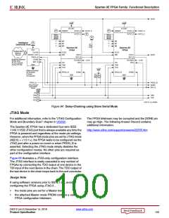
Slave Serial Mode
For additional information, refer to the “Slave Serial Mode”
chapter in UG332.
The intelligent host starts the configuration process by
pulsing PROG_B and monitoring that the INIT_B pin goes
High, indicating that the FPGA is ready to receive its first
data. The host then continues supplying data and clock
signals until either the DONE pin goes High, indicating a
successful configuration, or until the INIT_B pin goes Low,
indicating a configuration error. The configuration process
requires more clock cycles than indicated from the
configuration file size. Additional clocks are required during
the FPGA’s start-up sequence, especially if the FPGA is
programmed to wait for selected Digital Clock Managers
(DCMs) to lock to their respective clock inputs (see
Start-Up, page 106).
In Slave Serial mode (M[2:0] = <1:1:1>), an external host
such as a microprocessor or microcontroller writes serial
configuration data into the FPGA, using the synchronous
serial interface shown in Figure 63. The serial configuration
data is presented on the FPGA’s DIN input pin with
sufficient setup time before each rising edge of the
externally generated CCLK clock input.
DS312 (v4.2) December 14, 2018
www.xilinx.com
Product Specification
97

 XILINX [ XILINX, INC ]