Spartan-3E FPGA Family: Functional Description
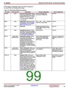
X-Ref Target - Figure 63
+1.2V
VCCINT
P
HSWAP
VCCO_0
VCCO_0
VCCO_2
V
Slave
Serial
Mode
V
‘1’
‘1’
‘1’
M2
M1
M0
Intelligent
V
Download Host
Spartan-3E
FPGA
VCC
Configuration
CLOCK
CCLK
DIN
Memory
Source
SERIAL_OUT
PROG_B
DONE
DOUT
INIT_B
• Internal memory
• Disk drive
VCCAUX
TDO
+2.5V
INIT_B
TDI
• Over network
• Over RF link
GND
TMS
TCK
+2.5V
• Microcontroller
• Processor
• Tester
PROG_B
DONE
GND
• Computer
PROG_B
Recommend
open-drain
driver
+2.5V
JTAG
TDI
TMS
TCK
TDO
DS312-2_54_082009
Figure 63: Slave Serial Configuration
The mode select pins, M[2:0], are sampled when the
FPGA’s INIT_B output goes High and must be at defined
logic levels during this time. After configuration, when the
FPGA’s DONE output goes High, the mode pins are
available as full-featured user-I/O pins.
Voltage Compatibility
V
Most Slave Serial interface signals are within the
FPGA’s I/O Bank 2, supplied by the VCCO_2 supply input.
The VCCO_2 voltage can be 3.3V, 2.5V, or 1.8V to match
the requirements of the external host, ideally 2.5V. Using
3.3V or 1.8V requires additional design considerations as
the DONE and PROG_B pins are powered by the FPGA’s
P
Similarly, the FPGA’s HSWAP pin must be Low to
enable pull-up resistors on all user-I/O pins or High to
disable the pull-up resistors. The HSWAP control must
remain at a constant logic level throughout FPGA
configuration. After configuration, when the FPGA’s DONE
output goes High, the HSWAP pin is available as
full-featured user-I/O pin and is powered by the VCCO_0
supply.
2.5V V
supply. See XAPP453: The 3.3V
CCAUX
Configuration of Spartan-3 FPGAs for additional
information.
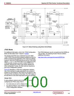
Daisy-Chaining
If the application requires multiple FPGAs with different
configurations, then configure the FPGAs using a daisy
chain, as shown in Figure 64. Use Slave Serial mode
(M[2:0] = <1:1:1>) for all FPGAs in the daisy-chain. After
the lead FPGA is filled with its configuration data, the lead
DS312 (v4.2) December 14, 2018
www.xilinx.com
Product Specification
98

 XILINX [ XILINX, INC ]