Philips Semiconductors
Preliminary specification
320 macrocell SRAM CPLD
PZ3320C/PZ3320N
breaking the paradigm that to have low power, you must have low
performance. This also makes it possible to manufacture high density
CPLDs like the PZ3320 that consume a fraction of the power of
TotalCMOS Design Technique
for Fast Zero Power
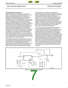
Philips is the first to offer a TotalCMOS CPLD, both in process
technology and design technique. Philips employs a cascade of
CMOS gates to implement its product terms instead of the traditional
sense amp approach. This CMOS gate implementation allows Philips
to offer CPLDs which are both high performance and low power,
competing devices. Refer to Figure 6 and Table 2 showing the I vs.
DD
Frequency of the PZ3320 TotalCMOS CPLD (data estimated with 20
16-bit counters @ 3.3V, 25°C).
500
I
DD
(mA)
450
400
350
300
250
200
150
100
50
0
0
20
40
60
80
100
120
FREQUENCY (MHz)
SP00657
Figure 6.
I vs. Frequency @ V = 3.3V, 25°C
DD DD
Table 2. I vs. Frequency
DD
V
DD
= 3.3V
FREQUENCY (MHz)
0
1
20
50
40
60
80
200
100
250
120
300
Typical I (mA)
0.1
4.1
100
150
DD
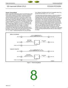
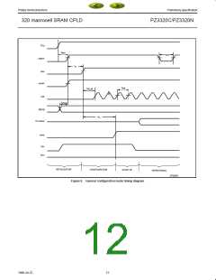
There are no on-chip pull-down structures associated with dedicated
pins used for device configuration or special device functions like
global reset and global 3-state. Philips recommends that these pins
be terminated consistent with the description given in Table 9.
Philips recommends the use of weak pull-up and pull-down resistors
for terminating these pins. These pins can be directly connected to
Terminations
The CoolRunnert PZ3320C/PZ3320N CPLDs are TotalCMOSt
devices. As with other CMOS devices, it is important to consider
how to properly terminate unused inputs and I/O pins when
fabricating a PC board. Allowing unused inputs and I/O pins to float
can cause the voltage to be in the linear region of the CMOS input
structures, which can increase the power consumption of the device.
It can also cause the voltage on a configuration pin to float to an
unwanted voltage level, interrupting device operation.
V
CC
or GND, but using the external pull-up resistors maintains
maximum design flexibility.
When using the JTAG Boundary Scan functions, it is recommended
that 10k pull-up resistors be used on the tdi, tdo, tck, and trstn pins.
The tdo signal pin can be left floating unless it is connected to the tdi
of another device. Letting these signals float can cause the voltage
on tms to come close to ground, which could cause the device to
enter JTAG/ISP mode at unspecified times.
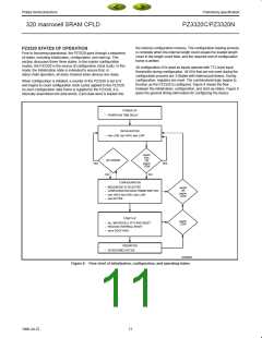
The PZ3320C/PZ3320N CPLDs have programmable on-chip
pull-down resistors on each I/O pin. These pull-downs are
automatically activated by the fitter software for all unused I/O pins.
Note that an I/O macrocell used as buried logic that does not have
the I/O pin used for input is considered to be unused, and the
pull-down resistors will be turned on. We recommend that any
unused I/O pins on the PZ3320C/PZ3320N device be left
unconnected.
9
1998 Jul 22

 XILINX [ XILINX, INC ]