Philips Semiconductors
Preliminary specification
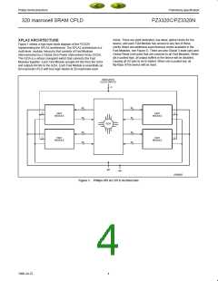
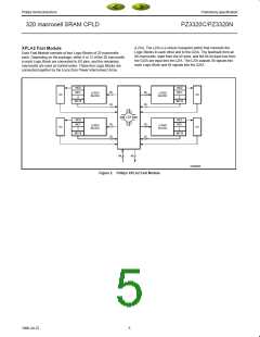
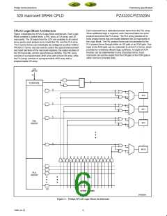
320 macrocell SRAM CPLD
PZ3320C/PZ3320N
from a different Fast Module would have a propagation delay of t
plus the fixed GZIA delay, or 7.5 + 4.0 = 11.5ns.
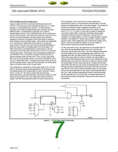
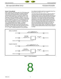
Simple Timing Model
PD
Figure 5 shows the PZ3320 timing model. The PZ3320 timing model
is very simple compared to the models of competing architectures.
There are three main timing parameters: the pin-to-pin delay for
This simple timing model allows designers to determine whether or
not the device will meet system timing specifications up front. In
competing devices, the user is unable to determine if the design will
meet system timing requirements until after the design has been fit
into the device. This is because the timing models of competing
architectures are very complex and include such things as timing
dependencies on the number of parallel expanders borrowed, the
fan-out of a signal, the varying number of X and Y routing channels
used, etc. The simplicity of the PZ3320 timing model gives you
pin-to-pin delay information before the design is set. Further, the
timing in the PZ3320 device will not vary with place and route
iterations caused by design changes. This allows the PZ3320 device
to meet your timing requirements even when you make changes to
the design.
combinatorial logic functions (t ), the input pin to register set up
PD
time (t ), and the register clock to valid output time (t ). As the
SU
CO
model shows, timing is only dependent on whether or not you use
the PLA array, and whether or not the logic function is created within
a single Fast Module or uses the GZIA. The timing starts with a set
time for t and t through the PAL array in a Fast Module, and
PD
SU
there are fixed delays added for use of the PLA array or the GZIA.
The t timing specification never changes. For example, a
CO
combinatorial logic function of four or fewer product terms
constructed from inputs within the same logic block would have a
t
delay of 7.5ns. If the logic function were more than four product
PD
terms wide, the delay would be t plus the fixed PLA delay, or
7.5 + 1.5 = 9.0ns. A function that used the PAL array and inputs
PD
Within a Fast Module:
t
= COMBINATORIAL PAL
PD_PAL
t
= COMBINATORIAL PAL + PLA
PD_PLA
INPUT PIN
OUTPUT PIN
OUTPUT PIN
REGISTERED
t
= PAL
= PAL + PLA
REGISTERED
SU_PAL
t
t
SU_PLA
CO
INPUT PIN
D
Q
GLOBAL CLOCK PIN
Using the Global ZIA:
t
= COMBINATORIAL PAL + GZD
PD_PAL
t
= COMBINATORIAL PAL + PLA ,+ GZD
PD_PLA
INPUT PIN
OUTPUT PIN
REGISTERED
= PAL + GZD
t
REGISTERED
SU_PAL
t
= PAL + PLA + GZD
t
SU_PLA
CO
INPUT PIN
D
Q
OUTPUT PIN
SP00591B
GLOBAL CLOCK PIN
Figure 5. PZ3320 Timing Model
8
1998 Jul 22

 XILINX [ XILINX, INC ]