Philips Semiconductors
Preliminary specification
320 macrocell SRAM CPLD
PZ3320C/PZ3320N
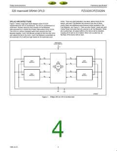
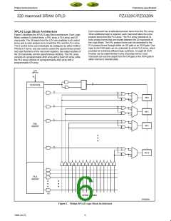
inside. There are eight dedicated, low-skew, global clocks for the
device; and each Fast Module has access to any two of these
clocks (there are additional asynchronous clocks available in the
Fast Modules, see Figure 3). There are also Global 3-state (gts) and
Global Reset (rstn) pins that are common to all Fast Modules. When
gts is pulled high, all output buffers in the device will be disabled,
causing all I/O pins to be tri-stated. When rstn is pulled low, all
flip-flops of the device will be reset.
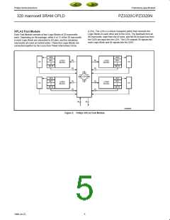
XPLA2 ARCHITECTURE
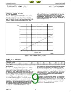
Figure 1 shows a high level block diagram of the PZ3320
implementing the XPLA2 architecture. The XPLA2 architecture is a
multi-level, modular hierarchy that consists of Fast Modules
interconnected by a Global Zero Power Interconnect Array (GZIA).
The GZIA is a virtual crosspoint switch that connects the Fast
Modules together. Each Fast Module accepts 64 bits from the GZIA
and outputs 64 bits to the GZIA. Each Fast Module is essentially an
80 macrocell CPLD with four logic blocks of 20 macrocells each
DEDICATED
CLOCK INPUTS
8
64
64
64
64
2
2
FAST
MODULE
FAST
MODULE
GZIA
64
64
64
64
2
2
FAST
MODULE
FAST
MODULE
gts
rstn
SP00655
Figure 1. Philips XPLA2 CPLD Architecture
4
1998 Jul 22

 XILINX [ XILINX, INC ]