Philips Semiconductors
Preliminary specification
320 macrocell SRAM CPLD
XCR3320
Xilinx has acquired the entire Philips CoolRunner Low Power CPLD Product Family. For
more technical or sales information, please see: www.xilinx.com
FEATURES
• 320 macrocell SRAM based CPLD
DESCRIPTION
The PZ3320 device is a member of the CoolRunner family of
high-density SRAM-based CPLDs (Complex Programmable Logic
Device) from Philips Semiconductors. This device combines high
speed and deterministic pin-to-pin timing with high density. The
PZ3320 uses the patented Fast Zero Power (FZP) design technique
that combines high speed and low power for the first time ever in a
CPLD. FZP allows the PZ3320 to have true pin-to-pin timing delays
of 7.5ns, and standby currents of 100 microamps without the need
for ‘turbo bits’ or other power down schemes. By replacing
conventional sense amplifier methods for implementing product
terms (a technique that has been used since the bipolar era) with a
cascaded chain of pure CMOS gates, both standby and dynamic
power are dramatically reduced when compared to other CPLDs.
The FZP design technique is also what allows Philips to offer a true
CPLD architecture in a high density device.
• Multiple power-up configuration modes
– Master serial
– Slave serial
– Master parallel-up
– Master parallel-down
– Slave parallel
– Synchronous peripheral
– Other modes available, contact Philips at 1–888–CoolPLD
• Configuration times of under 1.0 seconds
• IEEE 1149.1 compliant JTAG testing capability
– 5 pin JTAG interface
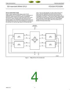
The Philips PZ3320C/PZ3320N devices use the new patent-pending
XPLA2 (eXtended Programmable Logic Array) architecture. This
architecture combines the best features of both PAL- and PLA-type
logic structures to deliver high speed and flexible logic allocation that
results in superior ability to make design changes with fixed pinouts.
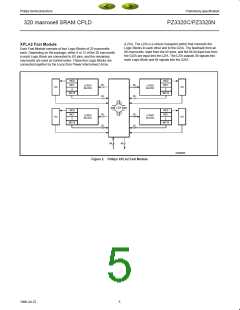
The XPLA2 architecture is constructed from 80 macrocell Fast
Modules that are connected together by an interconnect array.
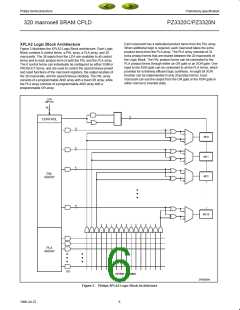
Within each Fast Module are four Logic Blocks of 20 macrocells
each. Each Logic Block contains a PAL structure with four dedicated
product terms for each macrocell. In addition, each Logic Block has
32 additional product terms in a PLA structure that can be shared
through a fully programmable OR array to any of the 20 macrocells.
This combination efficiently allocates logic throughout the Logic
Block, which increases device density and allows for design
changes without re-defining the pinout or changing the system
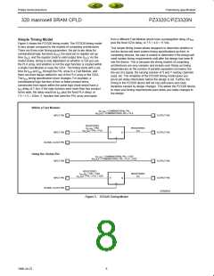
timing. The PZ3320 offers pin-to-pin propagation delays of 7.5ns
through the PAL array of a Fast Module; and if the PLA array is
used, an additional 1.5ns is added to the delay, no matter how many
PLA product terms are used. If the interconnect array between Fast
Modules is used, there is a second fixed addition to the propagation
delay of 4.0ns. This means that the worst case pin-to-pin
– IEEE 1149.1 TAP controller
• 3.3 volt device
• 5 V tolerant I/O
• Innovative XPLA2 Architecture combines extreme flexibility and
high speeds
• 8 synchronous clock networks with programmable polarity at
every macrocell
• Up to 32 asynchronous clocks support complex clocking needs
• Innovative XOR structure at every macrocell provides excellent
logic reduction capability
• Logic expandable to 36 product terms on a single macrocell
• PCI compliant (except for clamp diode to V rail due to 5 V
CC
tolerance)
• Advanced 0.35µ SRAM process
• Design entry and verification using industry standard and Philips
propagation delay within a fast module is 7.5 + 1.5 = 9.0 ns, and the
delay from any pin to any other pin across the entire chip is
7.5 + 4.0 = 11.5ns if only the PAL array is used, and
7.5 + 1.5 + 4.0 = 13.0ns if the PLA array is used. This deterministic
timing allows you to establish system timing before the logic design
is even started.
CAE tools
• Innovative Control Term structure provides either sum terms of
product terms in each logic block for:
– 3-State buffer control
– Asynchronous macrocell register reset/preset
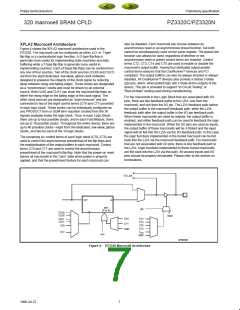
Each macrocell also has a two input XOR gate with the dedicated
PAL product terms on one input and the PLA product terms on the
other input. This patent-pending Versatile XOR structure allows for
very efficient logic optimization compared to competing XOR
structures that have only one product term as the second input to
the XOR gate. The Versatile XOR allows an 8 bit XOR function to be
implemented in only 20 product terms, compared to 65 product
terms for the traditional XOR approach.
• Global 3-State pin facilitates ‘bed of nails’ testing without
sacrificing logic resources
• Programmable slew rate control
• Small form factor packages with high I/O counts
• Available in commercial and industrial temperature ranges
The PZ3320 is SRAM-based, which means that it is configured at
power up by one of many different methods. The device may be
reconfigured any number of times. See the configuration section of
this data sheet for more information. The device supports the full
JTAG specification (IEEE 1149.1) through an industry standard
JTAG interface.
Table 1. PZ3320C/PZ3320N Features
PZ3320C/PZ3320N
Usable gates
10,000
192
Maximum inputs
Maximum I/Os
192
Number of macrocells
Propagation delay (ns)
Packages
320
7.5
160 pin LQFP
256 pin PBGA
2
1998 Jul 22

 XILINX [ XILINX, INC ]