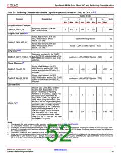
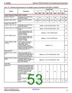
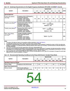
Spartan-6 FPGA Data Sheet: DC and Switching Characteristics
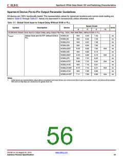
Spartan-6 Device Pin-to-Pin Output Parameter Guidelines
All devices are 100% functionally tested. The representative values for typical pin locations and normal clock loading are
listed in Table 61 through Table 67. Values are expressed in nanoseconds unless otherwise noted.
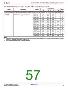
Table 61: Global Clock Input to Output Delay Without DCM or PLL
Speed Grade
Symbol
Description
Device
Units
-4
-3
-2
-1L
LVCMOS25 Global Clock Input to Output Delay using Output Flip-Flop, 12mA, Fast Slew Rate, without DCM or PLL
TICKOF
Global Clock and OUTFF without DCM or XC6SLX4
N/A
N/A
N/A
N/A
6.20
N/A
6.42
N/A
6.60
N/A
6.72
N/A
7.11
6.48
6.34
6.42
6.69
6.69
6.88
6.88
7.22
7.22
7.18
7.18
7.68
7.68
7.44
7.33
7.48
7.84
7.84
8.10
8.10
8.42
8.42
8.41
8.41
8.80
8.80
ns
ns
ns
ns
ns
ns
ns
ns
ns
ns
ns
ns
ns
PLL
XC6SLX9
XC6SLX16
XC6SLX25
XC6SLX25T
XC6SLX45
XC6SLX45T
XC6SLX75
XC6SLX75T
XC6SLX100
XC6SLX100T
XC6SLX150
XC6SLX150T
N/A
N/A
N/A
N/A
N/A
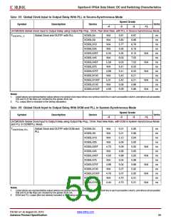
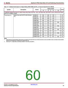
Notes:
1. Listed above are representative values where one global clock input drives one vertical clock line in each accessible column, and where all accessible
IOB and CLB flip-flops are clocked by the global clock net.
DS162 (v1.9) August 23, 2010
www.xilinx.com
Advance Product Specification
56

 XILINX [ XILINX, INC ]