Spartan-6 FPGA Data Sheet: DC and Switching Characteristics
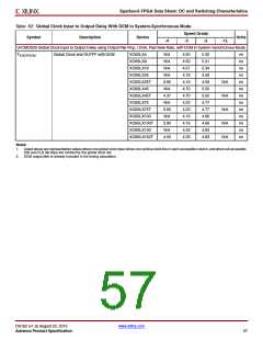
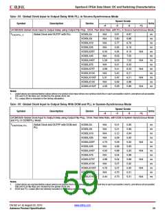
Table 62: Global Clock Input to Output Delay With DCM in System-Synchronous Mode
Speed Grade
-3 -2
LVCMOS25 Global Clock Input to Output Delay using Output Flip-Flop, 12mA, Fast Slew Rate, with DCM in System-Synchronous Mode.
Symbol
Description
Device
Units
-4
-1L
TICKOFDCM
Global Clock and OUTFF with DCM
XC6SLX4
N/A
N/A
N/A
N/A
3.95
N/A
4.37
N/A
3.90
N/A
3.90
N/A
4.03
4.50
4.50
4.57
4.18
4.18
4.70
4.70
4.23
4.23
4.16
4.16
4.33
4.33
5.32
5.31
5.34
4.59
4.59
5.50
5.50
4.77
4.77
4.66
4.66
4.83
4.83
ns
ns
ns
ns
ns
ns
ns
ns
ns
ns
ns
ns
ns
XC6SLX9
XC6SLX16
XC6SLX25
XC6SLX25T
XC6SLX45
XC6SLX45T
XC6SLX75
XC6SLX75T
XC6SLX100
XC6SLX100T
XC6SLX150
XC6SLX150T
N/A
N/A
N/A
N/A
N/A
Notes:
1. Listed above are representative values where one global clock input drives one vertical clock line in each accessible column, and where all accessible
IOB and CLB flip-flops are clocked by the global clock net.
2. DCM output jitter is already included in the timing calculation.
DS162 (v1.9) August 23, 2010
www.xilinx.com
Advance Product Specification
57

 XILINX [ XILINX, INC ]