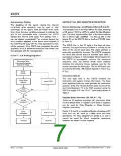
X9279
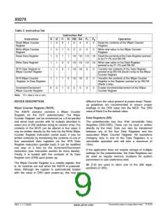
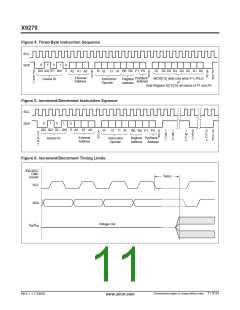
Figure 4. Three-Byte Instruction Sequence
SCL
0
1
0
1
0
0
SDA
ID1
S
T
A
R
T
ID3 ID2
ID0
A
C
K
I3
RB RA P1 P0
I0
A
C
K
D7 D6 D5 D4 D3 D2 D1 D0
A
C
K
S
T
I1
I2
A2 A1 A0
O
P
External
Address
Pot/Bank
Register
Address
WCR[7:0] valid only when P1=P0=0;
or
Device ID
Instruction
Opcode
Address
Data Register D[7:0] for all values of P1 and P0
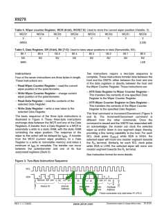
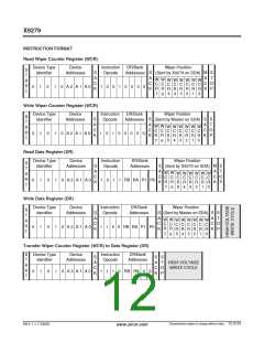
Figure 5. Increment/Decrement Instruction Squence
SCL
0
1
0
1
SDA
0
0
A2 A1 A0
ID3 ID2 ID1 ID0
Device ID
I3
I1
I2
I0
RB RA P1 P0
A
C
K
I
I
D
E
C
1
S
T
I
D
E
C
n
A
C
K
S
T
A
R
T
N
C
1
N
C
2
N
C
n
O
P
External
Address
Pot/Bank
Register
Address
Instruction
Opcode
Address
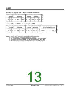
Figure 6. Increment/Decrement Timing Limits
INC/DEC
CMD
Issued
t
WRID
SCL
SDA
Voltage Out
V
/R
W
W
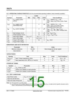
Characteristics subject to change without notice. 11 of 24
REV 1.1.7 2/6/03
www.xicor.com

 XICOR [ XICOR INC. ]