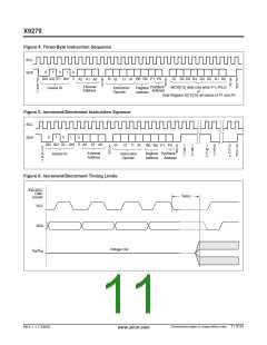
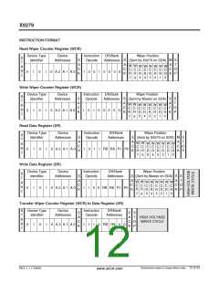
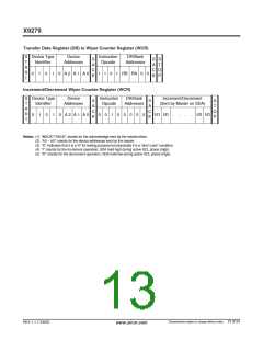
X9279
D.C. OPERATING CHARACTERISTICS (Over the recommended operating conditions unless otherwise specified.)
Limits
Symbol
Parameter
Min.
Typ.
Max.
Units
Test Conditions
= 400KHz; V = +6V;
SDA = Open; (for 2-Wire, Active, Read
and
I
I
I
V
supply current
(active)
3
mA
f
SCL
CC1
CC2
SB
CC
CC
V
supply current
(nonvolatile write)
5
5
mA
f
= 400KHz; V = +6V;
CC
SCL CC
SDA = Open; (for 2-Wire, Active,
Nonvolatile Write State only)
V
current (standby)
µA
V
= +6V; V = V or V
;
CC
CC
IN
SS
CC
SDA = V ; (for 2-Wire, Standby State
CC
only)
I
I
Input leakage current
Output leakage current
Input HIGH voltage
Input LOW voltage
10
10
µA
µA
V
V
= V to V
SS CC
LI
IN
V
= V to V
CC
LO
OUT
SS
V
V
V
V
V
x 0.7
V
+ 1
IH
CC
CC
–1
V
x 0.3
CC
V
IL
Output LOW voltage
Output HIGH voltage
0.4
V
I
= 3mA
OL
OL
OH
ENDURANCE AND DATA RETENTION
Parameter
Minimum endurance
Data retention
Min.
Units
100,000
100
Data changes per bit per register
years
CAPACITANCE
Symbol
Test
Input / Output capacitance (SDA)
Input capacitance (SCL, WP, A2, A1 and A0)
Max.
Units
pF
Test Conditions
= 0V
(6)
C
C
8
6
V
OUT
IN/OUT
(6)
pF
V
= 0V
IN
IN
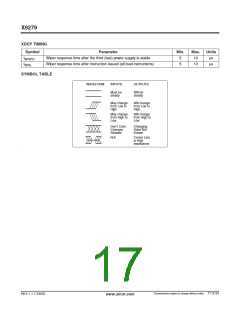
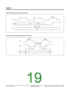
POWER-UP TIMING
Symbol
Parameter
V Power-up rate
CC
Min.
Max.
50
Units
V/ms
ms
(6)
t V
0.2
r
CC
(7)
t
t
Power-up to initiation of read operation
Power-up to initiation of write operation
1
PUR
(7)
50
ms
PUW
A.C. TEST CONDITIONS
Input Pulse Levels
V
x 0.1 to V x 0.9
CC
CC
Input rise and fall times
Input and output timing level
10ns
V
x 0.5
CC
Notes: (6) This parameter is not 100% tested
(7) t and t are the delays required from the time the (last) power supply (V -) is stable until the specific instruction can be
PUR
PUW
CC
issued.These parameters are periodically sampled and not 100% tested.
Characteristics subject to change without notice. 15 of 24
REV 1.1.7 2/6/03
www.xicor.com

 XICOR [ XICOR INC. ]