X9279
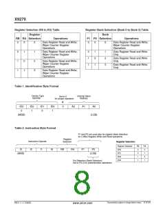
Register Selection (R0 to R3) Table
Register
Register Bank Selection (Bank 0 to Bank 3) Table
Bank
RB RA Selection
Operations
P1 P0 Selection
Operations
0
0
1
1
0
1
0
1
0
1
2
3
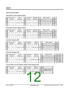
Data Register Read and Write;
Wiper Counter Register
Operations
0
0
0
Data Register Read and Write;
Wiper Counter Register
Operations
Data Register Read and Write;
Wiper Counter Register
Operations
0
1
1
1
0
1
1
2
3
Data Register Read and Write
Only
Data Register Read and Write
Only
Data Register Read and Write;
Wiper Counter Register
Operations
Data Register Read and Write
Only
Data Register Read and Write;
Wiper Counter Register
Operations
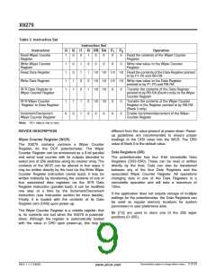
Table 1. Identification Byte Format
Device Type
Identifier
Internal Slave
Address
Set to 0
for proper operation
ID3
0
ID2
1
ID1
0
ID0
1
0
A2
A1
A0
(MSB)
(LSB)
Table 2. Instruction Byte Format
P1 and P0 are used also for register Bank Selection
for 2-Wire Register Write and Read operations
Register
Selection
Instruction Opcode
Register Selection
Register Selected
RB
0
RA
0
I3
I2
I1
I0
RB
RA
P1
P0
DR0
DR1
DR2
DR3
0
1
(MSB)
(LSB)
1
0
1
1
Pot Selection (Bank Selection)
Set to P0=0 for potentiometer operations
Characteristics subject to change without notice. 8 of 24
REV 1.1.7 2/6/03
www.xicor.com

 XICOR [ XICOR INC. ]