X9279
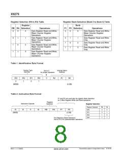
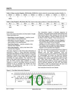
Table 4. Wiper counter Register, WCR (8-bit), WCR[7:0]: Used to store the current wiper position (Volatile, V).
WCR7
V
WCR6
V
WCR5
V
WCR4
V
WCR3
V
WCR2
V
WCR1
V
WCR0
V
(MSB)
(LSB)
Table 5. Data Register, DR (8-bit), Bit [7:0]: Used to store wiper positions or data (Nonvolatile, NV).
Bit 7
NV
Bit 6
NV
Bit 5
NV
Bit 4
NV
Bit 3
NV
Bit 2
NV
Bit 1
NV
Bit 0
NV
MSB
LSB
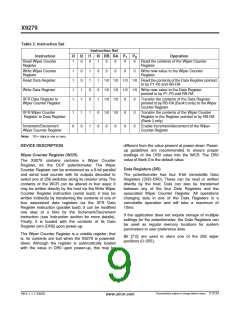
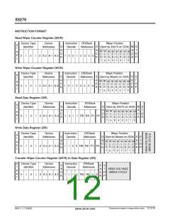
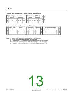
Instructions
Two instructions require a two-byte sequence to
complete. These instructions transfer data between the
host and the X9279; either between the host and one
of the data registers or directly between the host and
the Wiper Counter Register.These instructions are:
Four of the seven instructions are three bytes in length.
These instructions are:
– Read Wiper Counter Register – read the current
wiper position of the potentiometer,
– XFR Data Register to Wiper Counter Register –
This transfers the contents of one specified Data
Register to the Wiper Counter Register.
– Write Wiper Counter Register – change current
wiper position of the potentiometer,
– Read Data Register – read the contents of the
selected Data Register;
– XFR Wiper Counter Register to Data Register –
This transfers the contents of the Wiper Counter
Register to the specified Data Register.
– Write Data Register – write a new value to the
selected Data Register.
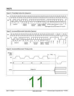
The final command is Increment/Decrement (Figure 5
and 6). The Increment/Decrement command is
different from the other commands. Once the
command is issued and the X9279 has responded with
an acknowledge, the master can clock the selected
wiper up and/or down in one segment steps; thereby,
providing a fine tuning capability to the host. For each
The basic sequence of the three byte instructions is
illustrated in Figure 4. These three-byte instructions
exchange data between the WCR and one of the Data
Registers. A transfer from a Data Register to a WCR is
essentially a write to a static RAM, with the static RAM
controlling the wiper position. The response of the
wiper to this action will be delayed by t
. A transfer
SCL clock pulse (t
) while SDA is HIGH, the
WRL
HIGH
from the WCR (current wiper position), to a Data
Register is a write to nonvolatile memory and takes a
selected wiper will move one resistor segment towards
the R terminal. Similarly, for each SCL clock pulse
H
minimum of t
to complete. The transfer can occur
while SDA is LOW, the selected wiper will move one
WR
between the potentiometer and one of its four
associated registers (Bank 0).
resistor segment towards the R terminal.
L
See Instruction format for more details.
Figure 3. Two-Byte Instruction Sequence
SCL
0
1
0
1
0
0
SDA
ID3 ID2 ID1 ID0
A2 A1 A0
S
T
A
R
T
0
A
C
K
RB RA P1
A
C
K
I3
I2
S
T
P0
I1 I0
O
P
Internal
Address
Device ID
Instruction
Opcode
Register
Address
Pot/Bank
Address
These commands only valid when P1=P0=0
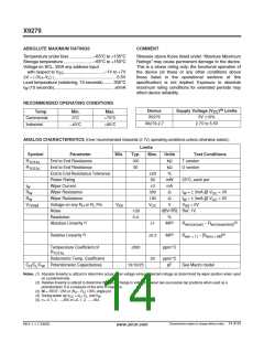
Characteristics subject to change without notice. 10 of 24
REV 1.1.7 2/6/03
www.xicor.com

 XICOR [ XICOR INC. ]