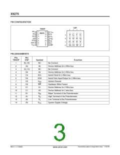
X9279
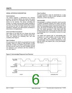
Acknowledge Polling
INSTRUCTION AND REGISTER DESCRIPTION
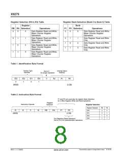
Device Addressing: Identification Byte ( ID and A)
The first byte sent to the X9279 from the host, following
a CS going HIGH to LOW, is called the Identification
byte. The most significant four bits of the slave address
are a device type identifier. The ID[3:0] bits is the
device ID for the X9279; this is fixed as 0101[B] (refer
to Table 1).
The disabling of the inputs, during the internal
nonvolatile write operation, can be used to take
advantage of the typical 5ms EEPROM write cycle
time. Once the stop condition is issued to indicate the
end of the nonvolatile write command the X9279
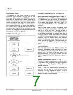
initiates the internal write cycle. ACK polling, Flow 1,
can be initiated immediately. This involves issuing the
start condition followed by the device slave address. If
the X9279 is still busy with the write operation no ACK
will be returned. If the X9279 has completed the write
operation an ACK will be returned and the master can
then proceed with the next operation.
The A[2:0] bits in the ID byte is the internal slave
address. The physical device address is defined by the
state of the A2-A0 input pins. The slave address is
externally specified by the user. The X9279 compares
the serial data stream with the address input state; a
successful compare of both address bits is required for
the X9279 to successfully continue the command
sequence. Only the device which slave address
matches the incoming device address sent by the
master executes the instruction. The A2-A0 inputs can
FLOW 1: ACK Polling Sequence
Nonvolatile Write
Command Completed
EnterACK Polling
be actively driven by CMOS input signals or tied to V
CC
or V
.
Issue
START
SS
Instruction Byte (I)
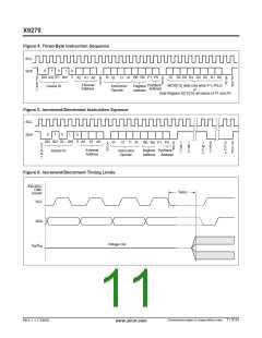
The next byte sent to the X9279 contains the
instruction and register pointer information. The three
most significant bits are used provide the instruction
opcode I [2:0]. The RB and RA bits point to one of the
four Data Registers. P0 is the POT selection; since the
X9279 is single POT, the P0=0. The format is shown in
Table 2.
Issue Slave
Issue STOP
Address
ACK
No
Returned?
Yes
Register Bank Selection (RB, RA, P1, P0)
Further
No
There are 16 registers organized into four banks. Bank
0 is the default bank of registers. Only Bank 0 registers
can be used for Data Register to Wiper Counter
Register operations.
Operation?
Yes
Banks 1, 2, and 3 are additional banks of registers (12
total) that can be used for 2-Wire write and read
operations. The Data Registers in Banks 1, 2, and 3
cannot be used for direct read/write operations
between the Wiper Counter Register.
Issue
Issue STOP
Instruction
Proceed
Proceed
Characteristics subject to change without notice. 7 of 24
REV 1.1.7 2/6/03
www.xicor.com

 XICOR [ XICOR INC. ]