X4043/45
Data Protection
Symbol Table
The following circuitry has been included to prevent
inadvertent writes:
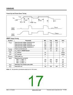
WAVEFORM
INPUTS
OUTPUTS
– The WEL bit must be set to allow write operations.
Must be
steady
Will be
steady
– The proper clock count and bit sequence is required
prior to the stop bit in order to start a nonvolatile write
cycle.
May change
from LOW
to HIGH
Will change
from LOW
to HIGH
– A three step sequence is required before writing into
the control register to change watchdog timer or
block lock settings.
May change
from HIGH
to LOW
Will change
from HIGH
to LOW
Don’t Care:
Changes
Allowed
Changing:
State Not
Known
– The WP pin, when held HIGH, prevents all writes to
the array and the control register.
N/A
Center Line
is High
Impedance
– Communication to the device is inhibited as a result
of a low voltage condition (V
< V
)any in-
CC
TRIP
progress communication is terminated.
– Block lock bits can protect sections of the memory
array from write operations.
Characteristics subject to change without notice. 13 of 25
REV 1.1.17 9/14/01
www.xicor.com

 XICOR [ XICOR INC. ]