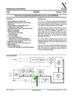
X1241 – Preliminary Information
PIN CONFIGURATION
X1, X2
The X1 and X2 pins are the input and output,
respectively, of an inverting amplifier that can be con-
figured for use as an on-chip oscillator. A 32.768kHz
quartz crystal is used. Recommended crystal is a Citizen
CFS-206. The crystal supplies a timebase for a clock/
oscillator. The internal clock can be driven by an
external signal on X1, with X2 left unconnected.
X1241
8-Pin SOIC
1
2
V
V
X1
X2
8
7
6
5
CC
Back
RESET
3
4
SCL
SDA
V
SS
Figure 1. Recommended Crystal Connection
X1241
8-Pin TSSOP
12pF
V
Back
SCL
SDA
1
2
8
7
6
5
V
CC
X1
X2
10M
V
SS
X1
X2
3
4
RESET
360K
68pF
PIN DESCRIPTIONS
Serial Clock (SCL)
POWER CONTROL OPERATION
The Power control circuit accepts a V
and a V
CC
BACK
The SCL input is used to clock all data into and out of
the device. The input buffer on this pin is always active
(not gated).
input. The power control circuit will switch to V
when V < V
BACK
– 0.2V. It will switch back to V
CC
CC
BACK
when V exceeds V
.
CC
BACK
Serial Data (SDA)
Figure 2. Power Control
SDA is a bidirectional pin used to transfer data into and
out of the device. It has an open drain output and may
be wire ORed with other open drain or open collector
outputs.The input buffer is always active (not gated).
V
CC
Internal
Voltage
V
BACK
V
= V
-0.2V
BACK
CC
An open drain output requires the use of a pull-up
resistor. The output circuitry controls the fall time of the
output signal with the use of a slope controlled pull-
down. The circuit is designed for 400kHz 2-wire inter-
face speeds.
REAL TIME CLOCK OPERATION
The Real Time Clock (RTC) uses an external, 32.768kHz
quartz crystal to maintain an accurate internal repre-
sentation of the year, month, day, date, hour, minute,
and seconds. The RTC has leap-year correction and a
century byte. The clock will also correct for months hav-
ing fewer than 31 days and will have a bit that controls
24-hour or AM/PM format. When the X1241 powers up
V
BACK
This input provides a backup supply voltage to the
device. V supplies power to the device in the
event the V supply fails.
BACK
CC
RESET Output—RESET
This is a reset signal output. This signal notifies a host
processor that the watchdog time period has expired or
that the voltage has dropped below a fixed V
after the loss of both V
and V
, the clock will not
CC
BACK
increment until at least one byte is written to the clock
register.
TRIP
threshold. It is an open drain active LOW output.
Characteristics subject to change without notice. 2 of 22
REV 1.1.3 2/13/01
www.xicor.com

 XICOR [ XICOR INC. ]