WM8983
Product Preview
CONTROL INTERFACE
SELECTION OF CONTROL MODE AND 2-WIRE MODE ADDRESS
The control interface can operate as either a 3-wire or 2-wire control interface. The MODE pin
determines the 2 or 3 wire mode as shown in Table 57.
The WM8983 is controlled by writing to registers through a serial control interface. A control word
consists of 16 bits. The first 7 bits (B15 to B9) are register address bits that select which control
register is accessed. The remaining 9 bits (B8 to B0) are data bits, corresponding to the 9 data bits
in each control register.
MODE
Low
INTERFACE FORMAT
2 wire
3 wire
High
Table 57 Control Interface Mode Selection
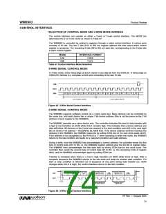
3-WIRE SERIAL CONTROL MODE
In 3-wire mode, every rising edge of SCLK clocks in one data bit from the SDIN pin. A rising edge on
CSB/GPIO latches in a complete control word consisting of the last 16 bits.
Figure 45 3-Wire Serial Control Interface
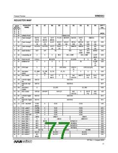
2-WIRE SERIAL CONTROL MODE
The WM8983 supports software control via a 2-wire serial bus. Many devices can be controlled by
the same bus, and each device has a unique 7-bit device address (this is not the same as the 7-bit
address of each register in the WM8983).
The WM8983 operates as a slave device only. The controller indicates the start of data transfer with
a high to low transition on SDIN while SCLK remains high. This indicates that a device address and
data will follow. All devices on the 2-wire bus respond to the start condition and shift in the next eight
bits on SDIN (7-bit address + Read/Write bit, MSB first). If the device address received matches the
address of the WM8983, the WM8983 responds by pulling SDIN low on the next clock pulse (ACK).
If the address is not recognised or the R/W bit is ‘1’ when operating in write only mode, the WM8983
returns to the idle condition and waits for a new start condition and valid address.
During a write, once the WM8983 has acknowledged a correct address, the controller sends the first
byte of control data (B15 to B8, i.e. the WM8983 register address plus the first bit of register data).
The WM8983 then acknowledges the first data byte by driving SDIN low for one clock cycle. The
controller then sends the second byte of control data (B7 to B0, i.e. the remaining 8 bits of register
data), and the WM8983 acknowledges again by pulling SDIN low.
Transfer is complete when there is a low to high transition on SDIN while SCLK is high. After a
complete sequence the WM8983 returns to the idle state and waits for another start condition. If a
start or stop condition is detected out of sequence at any point during data transfer (i.e. SDIN
changes while SCLK is high), the control interface returns to the idle condition.
DEVICE ADDRESS RD / WR
(7 BITS) BIT
ACK
(LOW)
CONTROL BYTE 1
(BITS 15 TO 8)
ACK
(LOW)
CONTROL BYTE 1
(BITS 7 TO 0)
ACK
(LOW)
SDIN
SCLK
START
STOP
register address and
1st register data bit
remaining 8 bits of
register data
Figure 46 2-Wire Serial Control Interface
PP Rev 1.1 August 2005
74
w

 WOLFSON [ WOLFSON MICROELECTRONICS PLC ]