Product Preview
WM8983
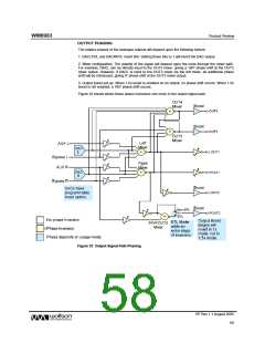
UNUSED ANALOGUE INPUTS/OUTPUTS
Whenever an analogue input/output is disabled, it remains connected to a voltage source (either
AVDD1/2 or 1.5xAVDD1/2 as appropriate) through a resistor. This helps to prevent pop noise when
the output is re-enabled. The resistance between the voltage buffer and the output pins can be
controlled using the VROI control bit. The default impedance is low, so that any capacitors on the
outputs can charge up quickly at start-up. If a high impedance is desired for disabled outputs, VROI
can then be set to 1, increasing the resistance to about 30kΩ.
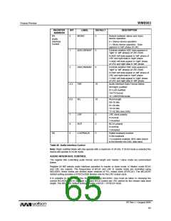
REGISTER
ADDRESS
BIT
LABEL
VROI
DEFAULT
DESCRIPTION
R49
0
0
VREF (AVDD1/2 or 1.5xAVDD/2) to
analogue output resistance
0: approx 1kΩ
1: approx 30 kΩ
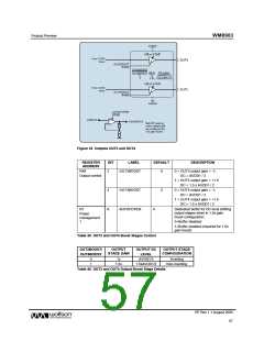
Table 44 Disabled Outputs to VREF Resistance
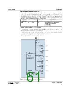
A dedicated buffer is available for biasing unused analogue I/O pins as shown in Figure 34. This
buffer can be enabled using the BUFIOEN register bit.
If the SPKBOOST, OUT3BOOST or OUT4BOOST bits are set then the relevant outputs will be tied
to the output of the DC level shift buffer at 1.5xAVDD/2 when disabled.
Figure 34 summarises the bias options for the output pins.
Figure 34 Unused Input/Output Pin Tie-off Buffers
PP Rev 1.1 August 2005
61
w

 WOLFSON [ WOLFSON MICROELECTRONICS PLC ]