Pre-Production
WM8904
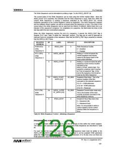
DEFAULT SEQUENCES
When the WM8904 is powered up, two Control Write Sequences are available through default
settings in both RAM and ROM memory locations. The purpose of these sequences, and the register
write required to initiate them, is summarised in Table 87. In both cases, a single register write will
initiate the sequence.
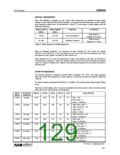
WSEQ START
INDEX
WSEQ FINISH
INDEX
PURPOSE
TO INITIATE
Write 0100h to
Register R111 (6Fh)
Write 0119h to
0 (00h)
22 (16h)
39 (27h)
Start-Up sequence
Shutdown sequence
25 (19h)
Register R111 (6Fh)
Table 87 Write Sequencer Default Sequences
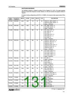
Note on Shutdown sequence: The instruction at Index Address 25 (19h) shorts the outputs
LINEOUTL and LINEOUTR. If the Line outputs are not in use at the time the sequence is run, then
the sequence could, instead, be started at Index Address 26.
Index addresses 0 to 31 may be programmed to users’ own settings at any time, as described in
“Programming a Sequence”. Users’ own settings remain in memory and are not affected by software
resets (i.e. writing to Register R0). However, any non-default sequences are lost when the device is
powered down.
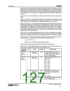
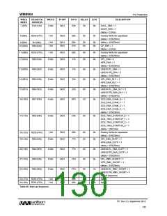
START-UP SEQUENCE
The Start-up sequence is initiated by writing 0100h to Register R111 (6Fh). This single operation
starts the Control Write Sequencer at Index Address 0 (00h) and executes the sequence defined in
Table 88.
For typical clocking configurations with MCLK=12.288MHz, this sequence takes approximately 300ms
to run.
Note that, for fast startup, step 18 may be overwritten with dummy data in order to achieve startup
within 50ms (see “Quick Start-Up and Shutdown”).
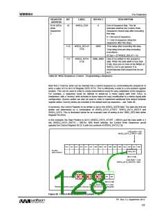
WSEQ
INDEX
REGISTER
ADDRESS
WIDTH
START
DATA
DELAY
EOS
DESCRIPTION
0 (00h)
5 bits
Bit 0
1Ah
0h
0b
ISEL = 10b
R4 (04h)
BIAS_ENA = 0
(delay = 0.5625ms)
VMID_BUF_ENA = 1
VMID_RES[1:0] = 11b
VMID_ENA = 1
1 (01h)
8 bits
Bit 0
47h
6h
0b
R5 (05h)
(delay = 4.5ms)
2 (02h)
3 (03h)
4 (04h)
2 bits
1 bit
Bit 1
Bit 0
Bit 0
01h
01h
03h
0h
0h
0h
0b
0b
0b
VMID_RES[1:0] = 01b
(delay = 0.5625ms)
BIAS_ENA = 1
R5 (05h)
R4 (04h)
R14 (0Eh)
(delay = 0.5625ms)
HPL_PGA_ENA = 1
HPR_PGA_ENA = 1
(delay = 0.5625ms)
LINEOUTL_PGA_ENA = 1
LINEOUTR_PGA_ENA = 1
(delay = 0.5625ms)
CLK_DSP_ENA = 1
(delay = 0.5625ms)
2 bits
5 (05h)
6 (06h)
2 bits
1 bit
Bit 0
Bit 1
03h
01h
0h
0h
0b
0b
R15 (0Fh)
R22 (16h)
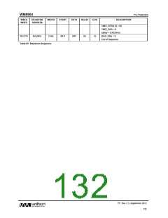
PP, Rev 3.3, September 2012
129
w

 WOLFSON [ WOLFSON MICROELECTRONICS PLC ]