WM8904
Pre-Production
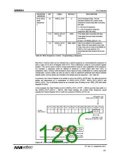
DESCRIPTION
REGISTER
ADDRESS
BIT
LABEL
DEFAULT
R110 (6Eh)
Write
Sequencer
2
End of Sequence flag. This bit
indicates whether the Control Write
Sequencer should stop after executing
this step.
14
WSEQ_EOS
0
0 = Not end of sequence
1 = End of sequence (Stop the
sequencer after this step).
Time delay after executing this step.
11:8
7:0
WSEQ_DELAY
[3:0]
0000
Total delay time per step (including
execution)=
62.5µs × (2^WSEQ_DELAY + 8)
Data to be written in this sequence
step. When the data width is less than
8 bits, then one or more of the MSBs of
WSEQ_DATA are ignored. It is
recommended that unused bits be set
to 0.
WSEQ_DATA
[7:0]
0000_0000
Table 86 Write Sequencer Control - Programming a Sequence
Note that a ‘Dummy’ write can be inserted into a control sequence by commanding the sequencer to
write a value of 0 to bit 0 of Register R255 (FFh). This is effectively a write to a non-existent register
location. This can be used in order to create placeholders ready for easy adaptation of the sequence.
For example, a sequence could be defined to power-up a mono signal path from DACL to
headphone, with a ‘dummy’ write included to leave space for easy modification to a stereo signal path
configuration. Dummy writes can also be used in order to implement additional time delays between
register writes. Dummy writes are included in the default start-up sequence – see Table 88.
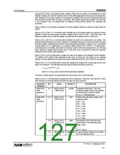
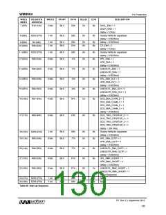
In summary, the Control Register to be written is set by the WSEQ_ADDR field. The data bits that are
written are determined by a combination of WSEQ_DATA_START, WSEQ_DATA_WIDTH and
WSEQ_DATA. This is illustrated below for an example case of writing to the VMID_RES field within
Register R5 (05h).
In this example, the Start Position is bit 01 (WSEQ_DATA_START = 0001b) and the Data width is 2
bits (WSEQ_DATA_WIDTH = 0001b). With these settings, the Control Write Sequencer would
updated the Control Register R5 [2:1] with the contents of WSEQ_DATA [1:0].
LSB position = b01
WSEQ_DATA_STARTn = 0001
b15 b14 b13 b12 b11 b10 b09 b08 b07 b06 b05 b04 b03 b02 b01 b00
R5 (05h)
VMID Control 0
VMID_RES
Data Width = 2 bits
WSEQ_DATA_WIDTHn = 0001
b07 b06 b05 b04 b03 b02 b01 b00
WSEQ_DATAn (8 bits)
WSEQ_DATA_WIDTHn = 2 bits.
Therefore, only the Least Significant 2 bits are valid. Bits 02 to 07 are discarded
Figure 68 Control Write Sequencer Example
PP, Rev 3.3, September 2012
128
w

 WOLFSON [ WOLFSON MICROELECTRONICS PLC ]