Pre-Production
WM8904
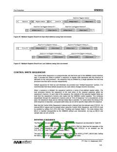
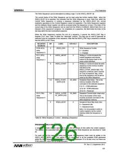
Having set the Index as described above, Register R109 must be written to (containing the Control
Register Address, the Start Bit Position and the Field Width applicable to this step of the sequence).
Also, Register R110 must be written to (containing the Register Data, the End of Sequence flag and
the Delay time required after this step is executed). After writing to these two registers, the next step
in the sequence may be programmed by updating WSEQ_WRITE_INDEX and repeating the
procedure.
WSEQ_ADDR is an 8-bit field containing the Control Register Address in which the data should be
written.
WSEQ_DATA_START is a 4-bit field which identifies the LSB position within the selected Control
Register to which the data should be written. Setting WSEQ_DATA_START = 0100 will cause 1-bit
data to be written to bit 4. With this setting, 4-bit data would be written to bits 7:4 and so on.
WSEQ_DATA_WIDTH is a 3-bit field which identifies the width of the data block to be written. This
enables selected portions of a Control Register to be updated without any concern for other bits within
the same register, eliminating the need for read-modify-write procedures. Values of 0 to 7 correspond
to data widths of 1 to 8 respectively. For example, setting WSEQ_DATA_WIDTH = 010 will cause a
3-bit data block to be written. Note that the maximum value of this field corresponds to an 8-bit data
block; writing to register fields greater than 8 bits wide must be performed using two separate
operations of the Control Write Sequencer.
WSEQ_DATA is an 8-bit field which contains the data to be written to the selected Control Register.
The WSEQ_DATA_WIDTH field determines how many of these bits are written to the selected
register; the most significant bits (above the number indicated by WSEQ_DATA_WIDTH) are ignored.
WSEQ_DELAY is a 4-bit field which controls the waiting time between the current step and the next
step in the sequence. The total delay time per step (including execution) is given by:
T = k × (2 WSEQ_DELAY + 8)
where k = 62.5s (under recommended operating conditions)
This gives a useful range of execution/delay times from 562s up to 2.048s per step.
WSEQ_EOS is a 1-bit field which indicates the End of Sequence. If this bit is set, then the Control
Write Sequencer will automatically stop after this step has been executed.
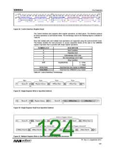
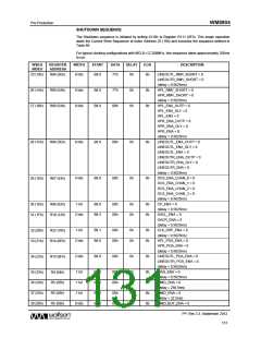
REGISTER
ADDRESS
BIT
LABEL
DEFAULT
DESCRIPTION
R108 (6Ch)
Write
Sequencer
0
Sequence Write Index. This is the
memory location to which any updates
to R109 and R110 will be copied.
4:0
WSEQ_WRITE
_INDEX [4:0]
0_0000
0 to 31 = RAM addresses
R109 (6Dh)
Write
Width of the data block written in this
sequence step.
14:12
WSEQ_DATA_
WIDTH [2:0]
000
Sequencer
1
000 = 1 bit
001 = 2 bits
010 = 3 bits
011 = 4 bits
100 = 5 bits
101 = 6 bits
110 = 7 bits
111 = 8 bits
Bit position of the LSB of the data
block written in this sequence step.
11:8
7:0
WSEQ_DATA_
START [3:0]
0000
0000 = Bit 0
…
1111 = Bit 15
Control Register Address to be written
to in this sequence step.
WSEQ_ADDR
[7:0]
0000_0000
PP, Rev 3.3, September 2012
127
w

 WOLFSON [ WOLFSON MICROELECTRONICS PLC ]