Pre-Production
WM8904
CONTROL INTERFACE
The WM8904 is controlled by writing to registers through a 2-wire serial control interface. Readback is
available for all registers, including Chip ID, power management status and GPIO status.
Note that, if it cannot be assured that MCLK is present when accessing the register map, then it is
required to set CLK_SYS_ENA = 0 to ensure correct operation. See “Clocking and Sample Rates” for
details of CLK_SYS_ENA.
The WM8904 is a slave device on the control interface; SCLK is a clock input, while SDA is a bi-
directional data pin. To allow arbitration of multiple slaves (and/or multiple masters) on the same
interface, the WM8904 transmits logic 1 by tri-stating the SDA pin, rather than pulling it high. An
external pull-up resistor is required to pull the SDA line high so that the logic 1 can be recognised by
the master.
In order to allow many devices to share a single 2-wire control bus, every device on the bus has a
unique 8-bit device ID (this is not the same as the 8-bit address of each register in the WM8904). The
WM8904 device ID is 0011 0100 (34h). The LSB of the device ID is the Read/Write bit; this bit is set
to logic 1 for “Read” and logic 0 for “Write”.
The WM8904 operates as a slave device only. The controller indicates the start of data transfer with a
high to low transition on SDA while SCLK remains high. This indicates that a device ID, register
address and data will follow. The WM8904 responds to the start condition and shifts in the next eight
bits on SDA (8-bit device ID including Read/Write bit, MSB first). If the device ID received matches
the device ID of the WM8904, then the WM8904 responds by pulling SDA low on the next clock pulse
(ACK). If the device ID is not recognised or the R/W bit is ‘1’ when operating in write only mode, the
WM8904 returns to the idle condition and waits for a new start condition and valid address.
If the device ID matches the device ID of the WM8904, the data transfer continues as described
below. The controller indicates the end of data transfer with a low to high transition on SDA while
SCLK remains high. After receiving a complete address and data sequence the WM8904 returns to
the idle state and waits for another start condition. If a start or stop condition is detected out of
sequence at any point during data transfer (i.e. SDA changes while SCLK is high), the device returns
to the idle condition.
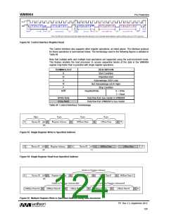
The WM8904 supports the following read and write operations:
Single write
Single read
Multiple write using auto-increment
Multiple read using auto-increment
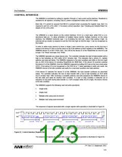
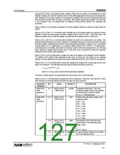
The sequence of signals associated with a single register write operation is illustrated in Figure 61.
Figure 61 Control Interface Register Write
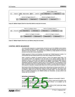
The sequence of signals associated with a single register read operation is illustrated in Figure 62.
PP, Rev 3.3, September 2012
123
w

 WOLFSON [ WOLFSON MICROELECTRONICS PLC ]