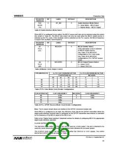
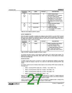
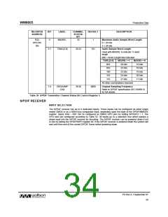
WM8805
Production Data
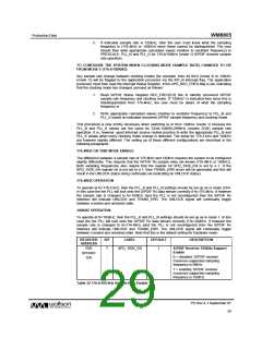
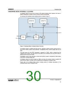
HARDWARE MODE INTERNAL CLOCKING
In hardware mode, the user has no access to the internal clocking control registers and hence a
default configuration is loaded at reset to provide maximum functionality.
An overview of the hardware mode clocking scheme is shown in Figure 17.
Figure 17 Hardware Mode Clocking Scheme Overview
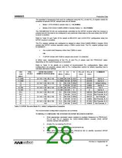
The S/PDIF receiver is enabled and hence the PLL operates in S/PDIF receiver mode and all PLL
and S/PDIF receiver control is fully automatic. All supported S/PDIF receiver sample rates can be
used.
The clock source for the S/PDIF transmitter is selected by TXSRC, which is latched from the
CSB/GPO2 pin at reset. The clock source for the MCLK pin is selected by the AIF_MS bit which is
latched from the SCLK pin at reset.
FREQMODE control is fully automatic to ensure that the MCLK output is maintained at 256fs relative
to the S/PDIF received sample rate.
In hardware mode, the OSCCLK must be 12MHz and hence the external crystal (or applied XIN
clock) must be 12MHz. No other OSCCLK frequencies are supported in hardware mode.
Please refer to the Software Mode Internal Clocking section for detailed descriptions of the
component blocks used in hardware mode.
PD Rev 4.1 September 07
30
w

 WOLFSON [ WOLFSON MICROELECTRONICS PLC ]