WM8805
Production Data
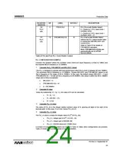
The specified f2 frequencies that must be configured using the PLL_N and PLL_K register values for
reception of specific S/PDIF sample rates are as follows:
•
•
Mode 1 (176.4/192kHz sample rate): f2 = 98.304MHz
Modes 2/3/4 (32/44.1/48/88.2/96kHz Sample Rates): f2 = 94.3104MHz
The FREQMODE[1:0] bits are automatically controlled by the S/PDIF receiver when the receiver is
enabled and do not need to be configured in any particular initial state by the user before the S/PDIF
receiver is enabled.
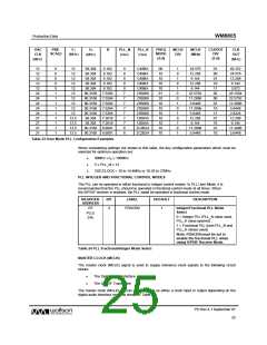
Refer to Table 23 and Table 28 for details of MCLKDIV and CLKOUTDIV configuration when the
S/PDIF receiver is enabled.
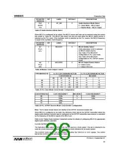
The PLL register settings are configured by default to allow 32/44.1/48/88.2/96kHz (modes 2/3/4)
sample rate S/PDIF receiver operation using a 12MHz crystal clock. The PLL register settings must
be updated if:
•
Any crystal clock frequency other than 12MHz is used.
OR
•
A S/PDIF stream with 192kHz sample rate (mode 1) is detected.
In either case, reprogramming of the PLL_N and PLL_K values (and the PRESCALE value,
depending on the crystal frequency) is necessary.
Refer to Table 31 for details of a number of recommended PLL configurations. Many other
configurations are possible; please refer to PLL Configuration section for details regarding how to
calculate alternative settings.
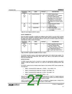
OSC
CLK
(MHz)
11.2896
11.2896
12
PRE-
SCALE
S/PDIF RECEIVER
SAMPLE RATE(S) (kHz)
F1
F2
R
PLL_N
PLL_K
COMMENT
(MHz)
(MHz)
(Hex)
(Hex)
0
0
0
0
0
0
1
1
1
1
1
1
32 / 44.1 / 48 / 88.2 / 96
11.2896 94.3104 8.3537
11.2896 98.304 8.7075
8
8
7
8
7
8
9
A
7
8
6
7
16A3B3
2D4766
36FD21
C49BA
2B3333
0
Set N, K
Set N, K
192
32 / 44.1 / 48 / 88.2 / 96
12
12
94.3104 7.8592
98.304 8.192
Default Setting
Set N, K
12
192
12.288
12.288
19.2
19.2
24
32 / 44.1 / 48 / 88.2 / 96
12.288 94.3104 7.675
12.288 98.304
Set K
192
8
Set N, K
32 / 44.1 / 48 / 88.2 / 96
9.6
9.6
94.3104 9.824
98.304 10.24
94.3104 7.8592
98.304 8.192
94.3104 6.986
98.304 7.2818
346C6A Set Prescale, N, K
F5C28 Set Prescale, N, K
192
32 / 44.1 / 48 / 88.2 / 96
12
36FD21
Set Prescale
24
192
32 / 44.1 / 48 / 88.2 / 96
192
12
C49BA Set Prescale, N, K
3F19E5 Set Prescale, N, K
27
13.5
13.5
27
1208A5
Set Prescale, K
Table 31 S/PDIF Receive Mode PLL Initial Configuration Examples
The recommended configuration sequences are as follows:
TO INITIALLY CONFIGURE THE SYSTEM FOR S/PDIF RECEIVER STARTUP:
1. Write appropriate calculated values (relative to oscillator frequency) to PRESCALE,
PLL_N and PLL_K registers for 32/44.1/48/88.2/96kHz (modes 2/3/4) S/PDIF
receiver sample rate operation.
2. Enable PLL by clearing PLLPD bit.
3. Enable S/PDIF receiver by clearing SPDIFRXPD bit.
4. Read S/PDIF Status Register REC_FREQ[1:0] bits to identify recovered S/PDIF
sample frequency and clocking mode.
PD Rev 4.1 September 07
28
w

 WOLFSON [ WOLFSON MICROELECTRONICS PLC ]