Production Data
WM8805
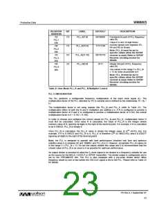
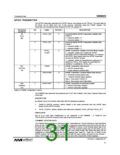
REGISTER
ADDRESS
BIT
LABEL
DEFAULT
DESCRIPTION
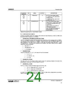
R7
PLL5
07h
5:4
CLKOUTDIV[1:0]
01
CLKOUT Divider Select
(Only valid when CLK1 is selected
as CLKOUT output source)
See Table 27 for CLKOUTDIV[1:0]
configuration in PLL user mode.
See Table 28 for CLKOUTDIV[1:0]
configuration in PLL S/PDIF receive
mode.
R8
PLL6
08h
3
4
CLKOUTSRC
CLKOUTDIS
1
1
CLKOUT Pin Source Select
0 = Select CLK1
1 = Select OSCCLK
CLKOUT Pin Disable
0 = Pin Disabled (Pin tri-stated)
1 = Pin Enabled
Table 29 Clock Output (CLKOUT) Control
S/PDIF TRANSMITTER
When the S/PDIF transmitter is enabled and configured (using TXSRC) to use the S/PDIF received
data, the S/PDIF transmitter is clocked from the CLK2 signal. When the transmitter’s data source is
the digital audio interface, the transmitter reference clock source is the MCLK signal at the MCLK
input/output pin. Refer to Table 30 for details.
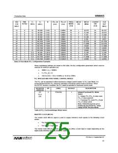
REGISTER
ADDRESS
BIT
LABEL
DEFAULT
DESCRIPTION
R21
SPDTX4
15h
6
TXSRC
1
S/PDIF Transmitter Data Source
0 = S/PDIF Received Data –
SPDIFTXCLK Source = CLK2
1 = Digital Audio Interface Received
Data – SPDIFTXCLK Source =
MCLK Input/Output Signal at MCLK
Pin
Table 30 S/PDIF Transmitter Data/MCLK Source Control
The S/PDIF transmitter requires a clock reference signal (either CLK2 or MCLK) when enabled. The
applied MCLK signal can be either128fs, 256fs, 384fs, 512fs, 768fs or 1152fs relative to the sample
rate of the transmitted data.
S/PDIF RECEIVER
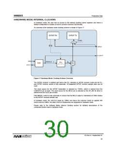
In S/PDIF receive mode, the PLL_N and PLL_K values are automatically modified by the S/PDIF
receiver to allow the receiver to use the PLL to lock on to and track the incoming S/PDIF data
stream.
The S/PDIF receiver has four clocking modes based on the incoming S/PDIF stream sample rate.
The modes are:
•
•
•
•
Mode 1: Incoming S/PDIF sample rate = 176.4kHz – 1% to 192kHz +1%
Mode 2: Incoming S/PDIF sample rate = 88.2kHz -1% to 96kHz +1%
Mode 3: Incoming S/PDIF sample rate = 44.1kHz -1% to 48kHz +1%
Mode 4: Incoming S/PDIF sample rate = 32kHz +/- 1%
Before the S/PDIF receiver is enabled, it is important that the PLL_N and PLL_K register values are
manually configured in a specific default state so that the S/PDIF receiver can correctly modify the
PLL_N and PLL_K values and hence establish correct PLL control.
The PLL_N and PLL_K register values must also be manually re-configured when a change of the
clocking mode is detected and the change is to mode 1 or from mode 1.
PD Rev 4.1 September 07
27
w

 WOLFSON [ WOLFSON MICROELECTRONICS PLC ]