WM8352
Production Data
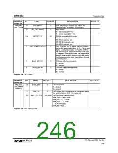
REGISTER
ADDRESS
BIT
LABEL
DEFAULT
DESCRIPTION
REFER TO
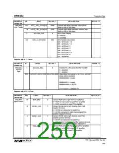
R68 (44h)
ADC Divider
11:8
7:4
3
ADCL_DAC_SVOL[3:0]
ADCR_DAC_SVOL[3:0]
ADCCLK_POL
0000
0000
0
Controls left digital side tone volume from -
36dB to 0dB in 3dB steps.
Controls right digital side tone volume from -
36dB to 0dB in 3dB steps.
ADC Clock Polarity
0 = Normal
1 = Inverted
2:0
ADC_CLKDIV[2:0]
000
ADC Sample rate divider
000 = SYSCLK / 1.0
001 = SYSCLK / 1.5
010 = SYSCLK / 2
011 = SYSCLK / 3
100 = SYSCLK / 4
101 = SYSCLK / 5.5
110 = SYSCLK / 6
111 = Reserved
Register 44h ADC Divider
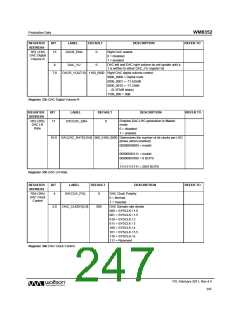
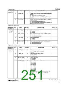
REGISTER
ADDRESS
BIT
LABEL
DEFAULT
DESCRIPTION
REFER TO
R70 (46h)
ADC LR
Rate
11
ADCLRC_ENA
0
Enables the LRC generation for the ADC
0 = disabled
1 = enabled
10:0 ADCLRC_RATE[10:0] 000_0100_0000 Determines the number of bit clocks per LRC
phase (when enabled)
00000000000 = invalid
...
00000000111 = invalid
00000001000 = 8 BCPS
…
11111111111 = 2047 BCPS
Register 46h ADC LR Rate
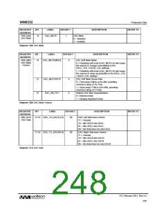
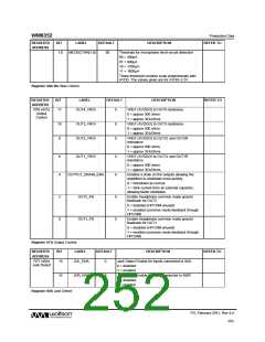
REGISTER
ADDRESS
BIT
LABEL
DEFAULT
DESCRIPTION
REFER TO
R72 (48h)
Input Control
10
IN2R_ENA
0
Connect IN2R pin to right channel input PGA
0 = IN2R not connected to input PGA amplifier
1 = IN2R connected to input PGA amplifier
9
8
2
IN1RN_ENA
IN1RP_ENA
IN2L_ENA
1
1
0
Connect IN1RN pin to right channel input PGA
negative terminal.
0 = IN1RN not connected to input PGA
1 = IN1RN connected to right channel input PGA
amplifier negative terminal.
Connect IN1RP pin to right channel input PGA
amplifier positive terminal.
0 = IN1RP not connected to input PGA
1 = right channel input PGA amplifier positive terminal
connected to IN1RP (constant input impedance)
Connect IN2L pin to left channel input PGA amplifier
0 = IN2L not connected to input PGA amplifier
1 = IN2L connected to input PGA amplifier
PD, February 2011, Rev 4.4
250
w

 WOLFSON [ WOLFSON MICROELECTRONICS PLC ]