WM8352
Production Data
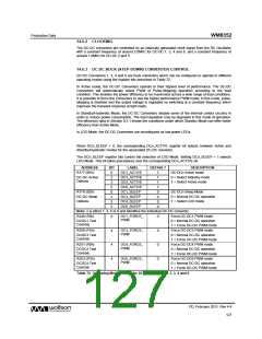
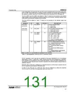
DC-DC Converters 1, 3, 4 and 6 can also be controlled by the device HIBERNATE bit, or by
hardware input signals L_PWR1, L_PWR2 and L_PWR3. Several GPIO pins can be assigned as
L_PWR pins. Each converter can be assigned to one of these three signals, or else to the device
HIBERNATE bit. The signals are active high and each converter’s response to the selected signal is
programmable as defined in Table 73.
Note that, when a GPIO pin is configured as a Hibernate input pin, and this input is asserted, then all
DC-DC Converters will be placed in Hibernate mode.
In order to use GPIO pins as L_PWR pins, they must be configured by setting the respective
GPn_FN, and GPn_DIR bits to the appropriate value (see Section 20).
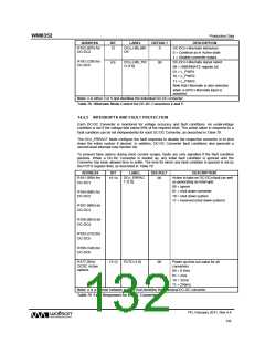
ADDRESS
BIT
LABEL
DEFAULT
DESCRIPTION
R182 (B6h) for
DC-DC1
14:12
DCn_HIB_M
ODE [2:0]
001
DC-DCn Hibernate behaviour:
000 = Use current settings (no change)
001 = Select voltage image settings
010 = Force standby mode
R188 (BCh) for
DC-DC3
011 = Force standby mode and voltage
image settings
R191 (BFh) for
DC-DC4
100 = Force LDO mode
101 = Force LDO mode and voltage
image settings
R197 (C5h) for
DC-DC6
110 = Reserved
111 = Disable output
DC-DCn Hibernate signal select
00 = HIBERNATE register bit
01 = L_PWR1
9:8
DCn_HIB_T
RIG [1:0]
00
10 = L_PWR2
11 = L_PWR3
Note that Hibernate is also selected
when a GPIO Hibernate input is
asserted.
Note: n is either 1, 3, 4 or 6 and identifies the individual DC-DC converter
Table 73 Low-Power Mode Control for DC-DC Converters 1, 3, 4 and 6
PD, February 2011, Rev 4.4
128
w

 WOLFSON [ WOLFSON MICROELECTRONICS PLC ]