WM8352
Production Data
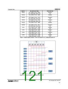
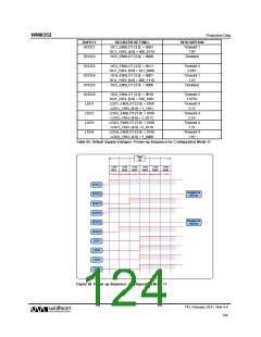
SUPPLY
REGISTER SETTING
DC1_ENSLOT [3:0] = 0001
DC1_VSEL [6:0] = 000_0110
DC2_ENSLOT [3:0] = 0000
DESCRIPTION
Timeslot 1
1.0V
DCDC1
DCDC2
DCDC3
DCDC4
DCDC5
DCDC6
LDO1
Disabled
DC3_ENSLOT [3:0] = 0011
DC3_VSEL [6:0] = 101_0000
DC4_ENSLOT [3:0] = 0001
DC4_VSEL [6:0] = 000_1110
DC5_ENSLOT [3:0] = 0000
Timeslot 3
2.85V
Timeslot 1
1.2V
Disabled
DC6_ENSLOT [3:0] = 0010
DC6_VSEL [6:0] = 010_1001
LDO1_ENSLOT [3:0] = 0100
LDO1_VSEL [4:0] = 1_1101
LDO2_ENSLOT [3:0] = 0100
LDO2_VSEL [4:0] = 1_0111
LDO3_ENSLOT [3:0] = 0100
LDO3_VSEL [4:0] = 0_0110
LDO4_ENSLOT [3:0] = 0100
LDO4_VSEL [4:0] = 1_0000
Timeslot 2
1.875V
Timeslot 4
3.1V
LDO2
Timeslot 4
2.5V
LDO3
Timeslot 4
1.2V
LDO4
Timeslot 4
1.8V
Table 69 Default Supply Voltages / Power-up Sequence for Configuration Mode 11
Start
Up
Time
Slot1
Time
Slot2
Time
Slot3
Time
Slot4
Time
Slot5
Time
Slot6
The time delay between each time slot is approximately 1.28ms.
DCDC1
DCDC2
DCDC3
DCDC4
DCDC5
DCDC6
LDO1
Disabled at
start-up
Disabled at
start-up
LDO2
LDO3
LDO4
Figure 68 Power-up Sequence - Configuration Mode 11
PD, February 2011, Rev 4.4
124
w

 WOLFSON [ WOLFSON MICROELECTRONICS PLC ]