Production Data
WM8352
In all configurations, the input pins VP2 and VP5 must be externally wired to one of the supply rails,
BATT or LINE. Using LINE has the advantage that the converters can operate when the battery is
flat, defective or absent. Note that VP2 and VP5 should not be connected to the USB supply rail.
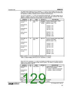
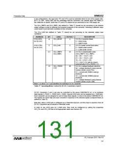
The DCn_RMPH and DCn_RMPL bits defined in Table 77 should be set according to the desired
output voltage in order to optimise the transient response of the converter. Selecting a different value
could result in sub-harmonic oscillation of the converter.
The DCn_ILIM bits defined in Table 77 should be set according to the intended output load
conditions.
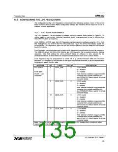
ADDRESS
R183 (B7h)
for DC-DC2
BIT
LABEL
DEFAULT
DESCRIPTION
DC-DCn Converter Mode
0 = boost mode
14
DCn_MODE
0
1 = switch mode
R192 (C0h)
for DC-DC5
6
DCn_ILIM
0
DC-DCn peak current limit select
0 = Higher peak current
1 = Lower peak current
DC-DCn compensation ramp
{DCn_RMPH, DCn_RMPL}
00 = 20V < VOUT ≤ 30V
01 = 10V < VOUT ≤ 20V
10 = 5V < VOUT ≤ 10V
4:3
DCn_RMPH
DCn_RMPL
01
11 = VOUT ≤ 5V (will be chosen
automatically if DCn_FBSRC=11)
1:0
DCn_FBSRC
00
DC-DCn voltage feedback selection
[1:0]
00 = voltage feedback (using external
resistor divider on pin FBn)
01 = current sink ISINKA used as
feedback
10 = current sink ISINKB used as
feedback
11 = voltage feedback (using internal
resistor divider on pin USB)
Note: n is either 2 or 5 and identifies the individual DC-DC converter
Table 77 Operating Mode Control for DC-DC Converters 2 and 5
DC-DC Converters 2 and 5 can also be controlled by the device HIBERNATE bit, or by hardware
input signals L_PWR1, L_PWR2 and L_PWR3. Several GPIO pins can be assigned as L_PWR pins.
Each converter can be assigned to one of these three signals, or else to the device HIBERNATE bit.
The signals are active high and each converter’s response to the selected signal is programmable as
defined in Table 78.
Note that, when a GPIO pin is configured as a Hibernate input pin, and this input is asserted, then all
DC-DC Converters will be placed in Hibernate mode.
In order to use GPIO pins as L_PWR pins, they must be configured by setting the respective
GPn_FN, and GPn_DIR bits to the appropriate value (see Section 20).
PD, February 2011, Rev 4.4
131
w

 WOLFSON [ WOLFSON MICROELECTRONICS PLC ]