Preliminary W91030B
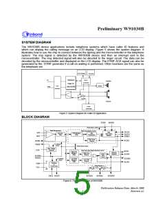
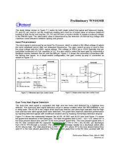
The diode bridge shown in Figure 7-1 works for both single ended ring signal and balanced ringing.
R1 and R2 are used to set the maximum loading and must be of equal value to achieve balanced
loading at both the tip and ring line. R1, R3 and R4 form a resistor divider to supply a reduced voltage
to the RNGDI input. The attenuation value is determined by the detection of minimal ring voltage and
maximum noise tolerance between tip/ring and ground.
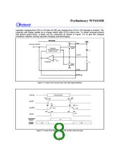
Input Pre-processor
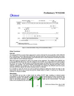
The input signal is processed by an Input Pre-Processor, which is added to the offset voltage to adjust
the input amplitude and to filter out unwanted frequencies. The gain control op-amp is used to bias
DD
the input voltage with the VREF signal voltage. The voltage of VREF pin is V /2 typically, this pin
had better connected a 0.1uF capacitor to VSS. It is also used to select the input gain by connecting a
feedback resistor between this pin and the INN pin. Figure 7-2 shows the necessary connections with
the tip/ring line inputs. In a single-ended configuration, the gain control op-amp is connected as
shown in Figure 7-3.
W91030B
W91030B
VREF
VREF
0.1 uF
R3
R4
0.1 uF
C1
C2
INP
INN
R1
R2
INP
INN
Tip
+
-
+
-
C
R1
Input
R5
GCFB
Ring
Voltage Gain
= R2 / R1
R2
GCFB
Voltage Gain
Differential Input Amplifier
A
V
C1 = C2
Av = R5 / R1
R1 = R2
R3 = (R4 R5) / (R4 +R5)
Input Impedance
2
2
Zin = 2 R1 + (1 / wC)
Figure 7-3 Single-ended Input Gain Control Circuit
Figure 7-2 Differential Input Gain Control Circuit
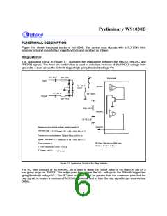
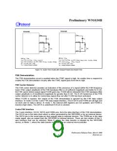
Dual Tone Alert Signal Detection
The dual tone alert signal is separated into high and low tones and detected by a high/low tone
detector. The dual tone alert signal detection circuit is always enabled when the W91030B/BS is not
in sleep state. The ALGR is the output of the dual tone detector and when high indicates that the high
tone and low tone alert signals have been detected. The guard time improves detection performance
by rejecting detected signals with insufficient duration and by masking momentary detection dropout.
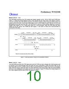
Figure 7-4 shows the relationship between the ALGR, ALGRC and ALGO pins and Figure 7-5 shows
REC
DP GP DP
the guard time waveform of the same pins. The total recognition time is t
the tone present detect time and t
= t + t , where t is
GP
is the tone present guard time. The tone present guard time is
SS
DD
the RC time constant with the capacitor discharging from V to V
( the ALGRC pin discharges
SS
DD
from V to V through a resistor). The capacitor will discharge rapidly via a discharge switch after
ABS
DA
GA
DA
ALGO returns high. The total absent time is t
= t + t , where t is the tone absent detect time
GA
and t is the tone absent guard time. The tone absent guard time is the RC time constant with the
Publication Release Date: March 2000
- 7 -
Revision A1

 WINBOND [ WINBOND ]