Preliminary W91030B
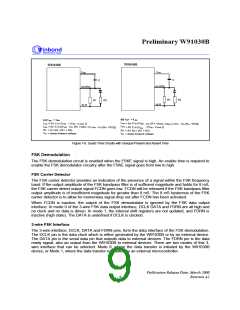
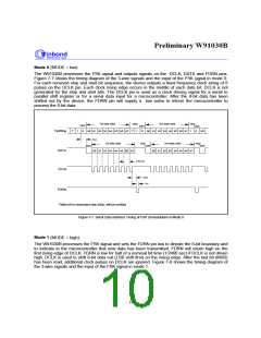
Mode 0
(MODE = low):
The W91030B processes the FSK signal and outputs signals on the DCLK, DATA and FDRN pins.
Figure 7-7 shows the timing diagram of the 3-wire signals and the input of the FSK signal in mode 0.
For each received stop and start bit sequence, the device outputs a fixed frequency clock string of 8
pulses on the DCLK pin. Each clock rising edge occurs in the middle of each data bit. DCLK is not
generated for the stop and start bits. The DCLK pin is used as a clock driving signal for a serial to
parallel shift register or for a serial data input for a microcontroller. After the 8-bit data has been
shifted out by the device, the FDRN pin will supply a low pulse to inform the microcontroller to
process the 8-bit data.
1st byte data
stop
2nd byte data
stop
start
start
0
start
0
Tip/Ring
1*
1
b0 b1 b2 b3 b4 b5 b6 b7 1*
1
b0 b1 b2 b3 b4 b5 b6 b7
1
0
b0
tIDD
1st byte data
stop
2nd byte data
stop
start
start
start
DATA
DCLK
b0 b1 b2 b3 b4 b5 b6 b7
b0 b1 b2 b3 b4 b5 b6 b7
DCLK0
1/f
tCRD
RL
t
FDRN
* Mark bit or redundant stop bit(s), will be omitted.
Figure 7-7. Serial Data Interface Timing of FSK Demodulation in Mode 0
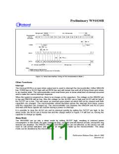
Mode 1
(MODE = high):
The W91030B processes the FSK signal and sets the FDRN pin low to denote the 8-bit boundary and
to indicate to the microcontroller that new data has been transmitted. FDRN will return high on the
first rising edge of DCLK. FDRN is low for half of a nominal bit time (1/2400 sec) if DCLK is not driven
high. DCLK is used to shift 8-bit data out (LSB shift first) on the rising edge. After the last bit (MSB)
has been read, additional clock pulses on DCLK are ignored. Figure 7-8 shows the timing diagram of
the 3-wire signals and the input of the FSK signal in mode 1.
- 10 -

 WINBOND [ WINBOND ]