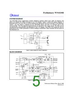
Preliminary W91030B
W91030B
W91030B
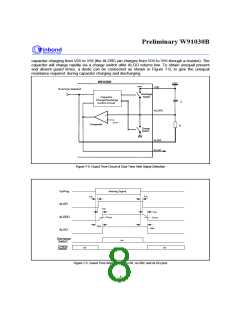
VDD
VDD
C
C
ALGRC
ALGRC
R2
R1
R2
R1
ALR
ALR
(b) tGP > t GA
> tGA
(a) t GP
t GP
tGA
= RP C ln [(VDD
= R1 C ln [VDD
t GP
tGA = R
RP
VD
/ (VDD -V
(RP
P
(R
/ R2)) / (VDD-V CPth
DD - VCPth )]
= R1 C ln [VDD
CPth )]
/ R2)) / (V CPth
-VD
/ (V
-V
/ R2))]
D (R P
P C ln [(VDD -VD
= R1 R2 / (R1 + R2)
= diode forward voltage
D
/ R2))]
-V (RP
RP
VD
= R1 R2 / (R1 + R2)
= diode forward voltage
Figure 7-6. Guard Time Circuits with Unequal Present and Absent Time
FSK Demodulation
The FSK demodulation circuit is enabled when the FSKE signal is high. An enable time is required to
enable the FSK demodulator circuitry after the FSKE signal goes from low to high.
FSK Carrier Detector
The FSK carrier detector provides an indication of the presence of a signal within the FSK frequency
band. If the output amplitude of the FSK bandpass filter is of sufficient magnitude and holds for 8 mS,
the FSK carrier detect output signal FCDN goes low. FCDN will be released if the FSK bandpass filter
output amplitude is of insufficient magnitude for greater than 8 mS. The 8 mS hysteresis of the FSK
carrier detector is to allow for momentary signal drop out after FCDN has been activated.
When FCDN is inactive, the output of the FSK demodulator is ignored by the FSK data output
interface. In mode 0 of the 3-wire FSK data output interface, DCLK DATA and FDRN are all high and
no clock and no data is driven. In mode 1, the internal shift registers are not updated, and FDRN is
inactive (high state). The DATA is undefined if DCLK is clocked.
3-wire FSK Interface
The 3-wire interface, DCLK, DATA and FDRN pins, form the data interface of the FSK demodulation.
The DCLK pin is the data clock which is either generated by the W91030B or by an external device.
The DATA pin is the serial data pin that outputs data to external devices. The FDRN pin is the data
ready signal, also an output from the W91030B to external devices. There are two modes of this 3-
wire interface that can be selected. Mode 0, where the data transfer is initiated by the W91030B
device, or Mode 1, where the data transfer is initiated by an external microcontroller.
Publication Release Date: March 2000
- 9 -
Revision A1

 WINBOND [ WINBOND ]