Preliminary W91030B
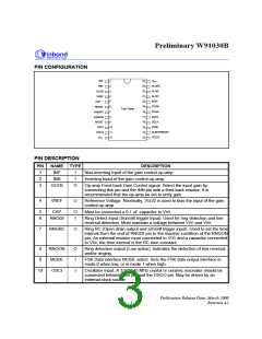
PIN CONFIGURATION
INP
INN
1
24
23
22
21
20
19
18
17
16
15
14
13
VDD
2
ALGRC
ALGR
3
GCFB
VREF
CAP
4
ALGO
5
INTN
6
FCDN
RNGDI
RNGRC
RNGON
MODE
OSCI
Top View
7
FDRN
8
DATA
9
DCLK
10
11
12
FSKE
OSCO
VSS
SLEEP/RESET
TEST2
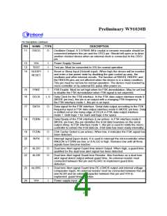
PIN DESCRIPTION
PIN
1
NAME TYPE
DESCRIPTION
INP
INN
I
I
Non-inverting Input of the gain control op-amp.
Inverting Input of the gain control op-amp.
2
3
GCFB
O
Op-amp Feed-back Gain Control signal. Select the input gain by
connecting this pin and the INN pin with a feed-back resistor. It is
recommended that the op-amp be set to unity gain.
DD
4
VREF
O
Reference Voltage. Nominally, V /2 is used to bias the input of the gain
control op-amp.
5
6
CAP
O
I
SS
m
Must be connected a 0.1 F capacitor to V
.
RNGDI
Ring Detect Input (Schmitt trigger input). Used for ring detection and line
reversal detection. Must maintain a voltage between V and V
DD
SS
.
7
RNGRC
O
Ring RC (Open drain output and schmitt trigger input). Used to set the time
interval from the end of RNGDI pin to the inactive condition of the RNGON
pin. An external resistor must connected to V and a capacitor connected
DD
SS
to V , the time interval is the RC time constant.
8
9
RNGON
MODE
OSCI
O
I
Ring detection output (Low active). Indicates the detection of line reversal
and/or ringing.
FSK Data interface MODE select. Sets the FSK data output interface in
mode 0 when low, or in mode 1 when high.
10
I
Oscillator Input. A 3.579545 MHz crystal or ceramic resonator should be
connected between this pin and the OSCO pin. May be driven by an
external clock source.
Publication Release Date: March 2000
- 3 -
Revision A1

 WINBOND [ WINBOND ]