Preliminary W91030B
SYSTEM DIAGRAM
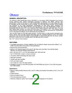
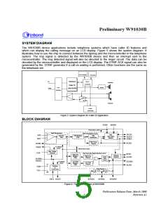
The W91030B device applications include telephone systems which have caller ID features and
which can display the calling message on an LCD display. Figure 5 shows the system diagram. It
illustrates how to use the chip to connect between the tip/ring and the microcontroller in the telephone
system. The ring signal is detected by the W91030B device and then an interrupt sent to the
microcontroller. The ring detected signal will also be directed to the ringer circuit. The data can be
decoded by the microcontroller and displayed on the LCD display. The DTMF ACK signal can also be
generated by the DTMF generator if a call on waiting is performed. Other functions are the same as
the telephone set.
LCD Display
Keypads
Winbond
Tip
Micro
Controller
Speaker
Caller ID
Line
Ringer
Ring
(W91030B)
Interface
Handset
DTMF
Generator
Figure 5. System Diagram for Caller ID Application
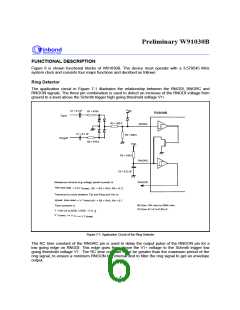
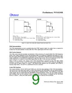
BLOCK DIAGRAM
MODE
FSKE
Power down control
Input Pre-processor
FSK Demodulation Circuit
DCLK
DATA
FDRN
FSK
Data Output
Interface
+
INP
Anti-alias
Filter
FSK Bandpass
Filter
FSK
Demodulator
-
INN
FSK Carrier
Detector
FCDN
GCFB
VREF
To internal
circuit
Power down control
Bias Voltage
Generator
CAP
Dual Tone Alert Signal Detection Circuit
INTN
High Tone
Bandpass
Filter
Interrupt
Generator
High Tone
Guard
ALGO
Detector
Time
SLEEP/
RESET
Circuit
ALGRC
ALGR
To internal
circuit
Low Tone
Bandpass
Filter
Low Tone
Detector
Oscillator
&
Clock Driver
VDD
VSS
Ring Detector
RNGRC
RNGDI
RNGON
OSCI
OSCO
Figure 6. The Block Diagram of W91030B
Publication Release Date: March 2000
Revision A1
- 5 -

 WINBOND [ WINBOND ]